Capacitor having microstructures

a microstructure, capacitor technology, applied in the direction of capacitors, fixed capacitor details, capacitors, etc., can solve the problems of difficult micromachining of capacitors, difficult to obtain large capacitance due to an increase in area, and difficult to obtain pillar-shaped bodies with uniform cross-sections. , to achieve the effect of improving the arbitrariness of electrode metal and dielectric material, improving the capacitance density, and simplifying the manufacturing process

Active Publication Date: 2011-03-08
TAIYO YUDEN KK
View PDF11 Cites 19 Cited by
  • Summary
  • Abstract
  • Description
  • Claims
  • Application Information

AI Technical Summary

Benefits of technology

[0009]The present invention was made with attention paid to the foregoing points. It is an object of one or more embodiment of the invention to provide a capacitor which can improve the capacitance density, can improve the arbitrariness of the electrode metal and the dielectric material, and / or can simplify the manufacturing process, while being compact, and, in another aspect, to provide a manufacturing method thereof. Further, it is another object of one or more embodiments of the invention to provide a capacitor capable of reducing ESL, and, in another aspect, to provide a manufacturing method thereof.
[0016]In accordance with an embodiment of the invention, a structure of an oxide base material including gaps for filling an electrode material therein is formed, and a first electrode and second electrodes are filled in the gaps. Then, a high permittivity material is filled in the gap part formed by removal of the oxide base material to obtain a dielectric substance (layer). Therefore, it is possible to achieve a high capacitance. Still further, the structure of the oxide base material is formed first, and then, the electrode material is filled in the gap part. This produces effects of increasing the selection of the electrode metal species, and simplifying the manufacturing process. Still further, the oxide base material is removed, and a high permittivity material is filled. Therefore, the selection of the dielectric material is enhanced, which allows the dielectric material to be changed according to the use thereof.
[0022]In accordance with an embodiment of the invention, on the surface of the oxide base material including an anodic oxide of a metal, and having a prescribed thickness, a pair of generally comb-shaped surface electrodes are formed such that the mutual tooth parts are alternately arranged in parallel at a prescribed interval. In addition, there are provided a plurality of generally pillar-shaped internal electrodes connected to the tooth parts at one ends thereof, and extending in the direction of thickness of the oxide base material on the other end side. In the gap part formed by removal of the oxide base material, a high permittivity material is filled, thereby to obtain a dielectric layer. For this reason, in addition to the foregoing effects, the effect of mutual cancelling of magnetic fields is enhanced by forming the surface electrodes in closest relation to each other on the same plane so that the current directions are opposite. This produces an effect of capable of reducing ESL.

Problems solved by technology

This entails a difficult problem that a configuration for preventing solution leakage must be considered, or other difficult problems.
This entails a difficult problem that design allowing for distortion due to a difference in thermal contraction between the electrode and the dielectric substance or the like must be adopted, and other difficult problems.
However, the background art described up to this point has the following problems.
However, micromachining thereof is difficult, which entails a problem that large capacitance due to an increase in area is difficult to attain.
Therefore, it is difficult to obtain pillar-shaped bodies with a uniform cross sectional shape and a desirable shape.
This entails a problem that it is difficult to attain a large capacitance by an increase in height of pillar-shaped bodies.
Therefore, it is difficult to increase the aspect ratio in a z direction (direction of thickness).
Therefore, it is difficult to increase the aspect ratio in a z direction.
Thus, unfavorably, with the electrode forming technology by etching, it is difficult to increase the aspect ratio in a z direction of the electrode part, and to increase the area defining the capacitance.

Method used


Image

  • Capacitor having microstructures
  • Capacitor having microstructures
  • Capacitor having microstructures

Examples


example 1

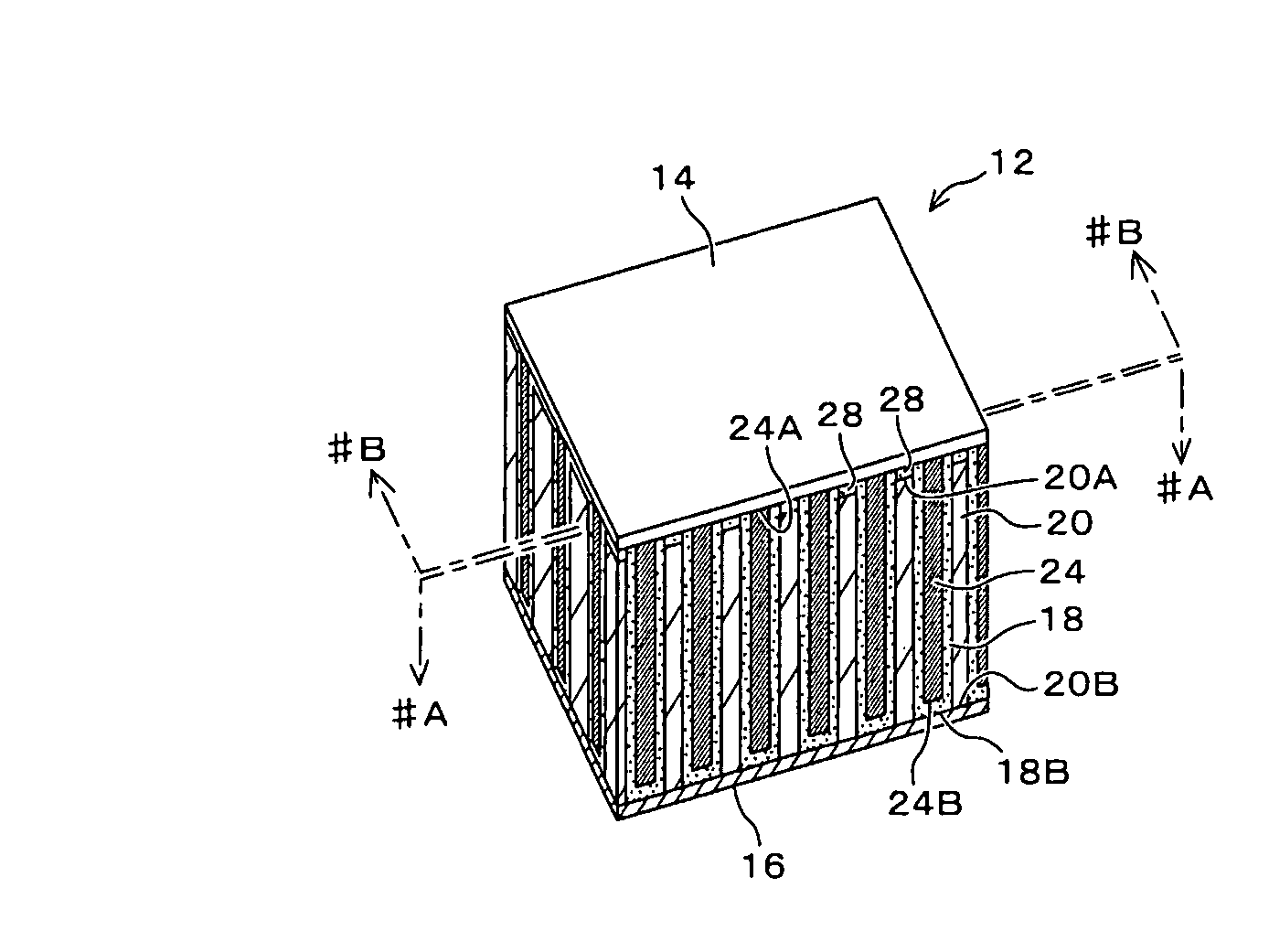
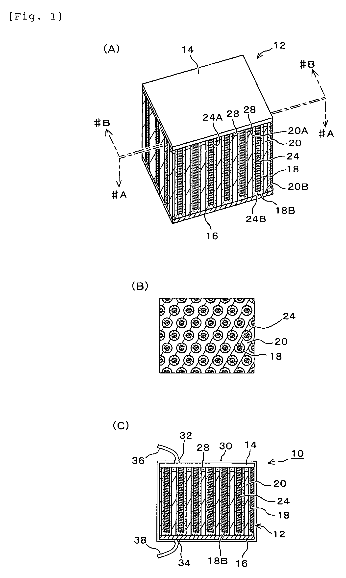
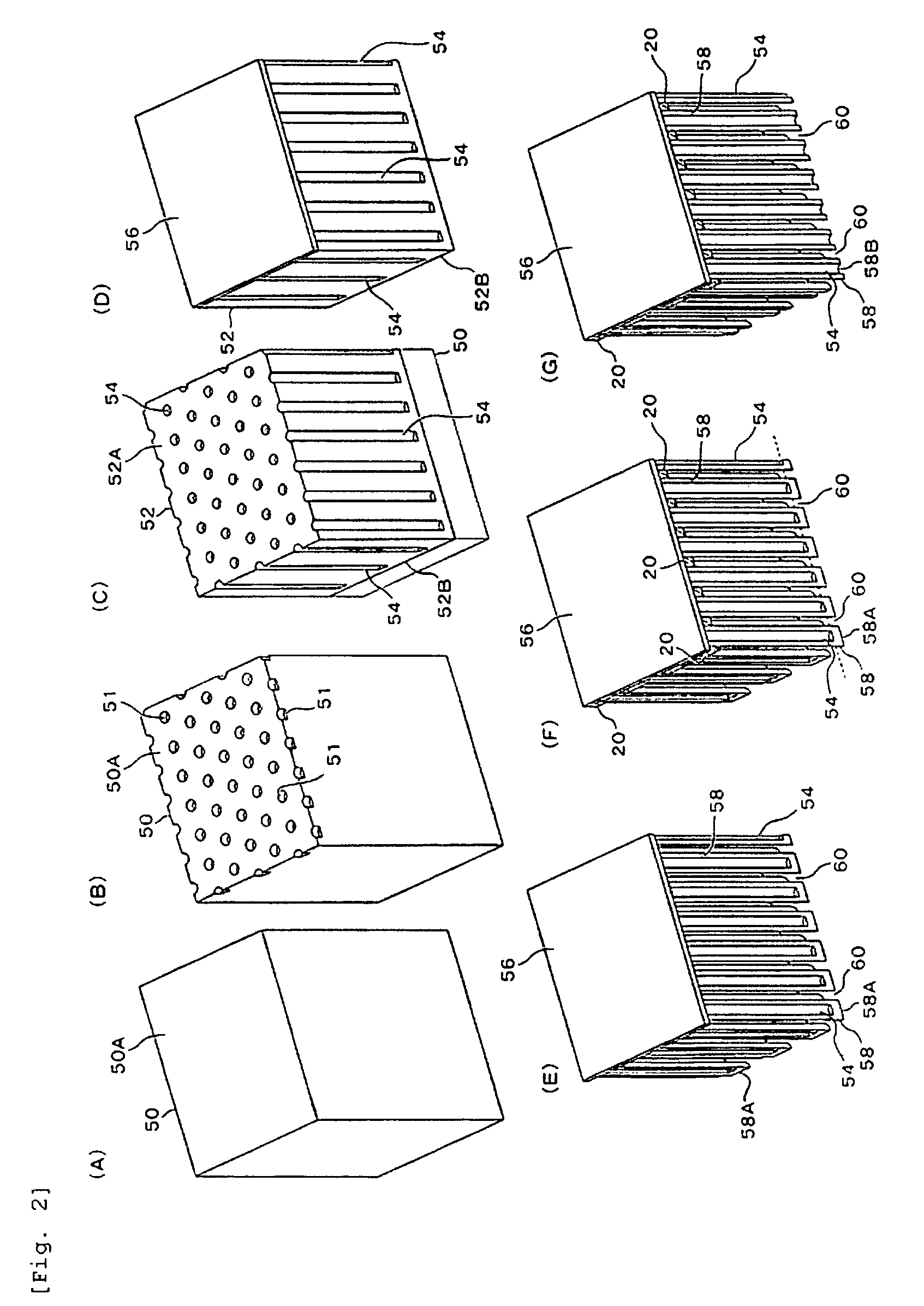
[0042]First, Example 1 of the invention will be described by reference to FIGS. 1A to 1C to 4A to 4C. FIG. 1A is a perspective view of the outward appearance of a capacitor element of this example. FIG. 1B is a cross sectional view of the capacitor element cut along line #A-#A, and seen from a direction of an arrow of FIG. 1A. FIG. 1C is a cross sectional view of the capacitor of this example, and corresponds to a cross sectional view cut along line #B-#B, and seen from a direction of an arrow of FIG. 1A. FIGS. 2A to 2G to 4C each show one example of a manufacturing step of this example.

[0043]A capacitor 10 of this example is configured with a capacitor element 12 as the center as shown in FIG. 1C. The capacitor element 12 includes a pair of conductor layers 14 and 16 facing each other at a prescribed distance, a plurality of generally tube-shaped dielectric substances 18, a first electrode 20 disposed between the plurality of the dielectric substances 18, and a plurality of second ...

example 2

[0057]Then, Example 2 of the invention will be described by reference to FIGS. 5A and 5B to 8A to 8C. FIG. 5A is a main cross sectional view of a capacitor element of this example. FIG. 5B is a cross sectional view of the capacitor element cut along line #C-#C, and seen from a direction of an arrow of FIG. 5A. FIGS. 6A to 6G to 8A to 8C each show one example of a manufacturing step of this example. As shown in FIGS. 5A and 5B, a capacitor element 100 of this example is configured as follows: a dielectric layer 106 including a high permittivity material is provided between a pair of opposing conductor layers 102 and 104; and first electrodes 108 and second electrodes 110 are disposed in a plurality of holes penetrating through the dielectric layer 106.

[0058]In this example, as shown in FIG. 5B, the arrangement is configured such that the second electrodes 110 are situated at the apexes of hexagons forming a honeycomb structure, and such that the first electrodes 108 are situated at t...

example 3

[0065]Then, by reference to FIGS. 9A and 9B to 11A to 11G, Example 3 of the invention will be described. FIG. 9A is a perspective view showing the electrode structure of a capacitor element of this example. FIG. 9B is a perspective view of an outward appearance of the capacitor of this example. FIGS. 10A to 10F and 11A to 11E are views each showing one example of the manufacturing step of this example. A capacitor 200 of this example includes a dielectric layer 204 having a prescribed thickness, a pair of generally comb-shaped surface electrodes 206 and 210 formed at a surface 204A of the dielectric layer 204, and a plurality of generally pillar-shaped internal electrodes 208 and 212 extending from the surface electrodes 206 and 210 toward the rear surface 204 B of the dielectric layer 204. On the dielectric layer rear surface 204B, if required, an insulator layer 214 is provided.

[0066]The dielectric layer 204 is formed of a high permittivity material. The internal electrodes 208 an...


PUM

PropertyMeasurementUnit
aspect ratioaaaaaaaaaa

Abstract

A capacitor element includes a pair of conductor layers, a plurality of generally tube-shaped dielectric substances, a first electrode outside the dielectric substances and second electrodes in the insides thereof, and insulation caps for insulating the first electrode from the conductor layer, wherein an electrode material is filled in gaps of a structure of an oxide base material resulting from anodic oxidation of a metal, and then, the structure is removed and replaced by a high permittivity material.

Description

BACKGROUND OF THE INVENTION[0001]1. Field of the Invention[0002]The present invention relates to a capacitor and a manufacturing method thereof. More particularly, it relates to the improvement of the capacitance density of a capacitor, reduction of ESL (Equivalent Series Inductance), the improvement of the arbitrariness of the electrode metal and the dielectric material in the configuration of a capacitor, and simplification of the manufacturing process of a capacitor.[0003]2. Description of Related Art[0004]As currently widely used capacitors, Al electrolytic capacitors and multi-layer ceramics capacitors are known. With Al electrolytic capacitors, an electrolyte is used. This entails a difficult problem that a configuration for preventing solution leakage must be considered, or other difficult problems. Whereas, multi-layer ceramics capacitors require sintering. This entails a difficult problem that design allowing for distortion due to a difference in thermal contraction between...

Claims


Application Information

Patent Timeline
Patent Type & Authority Patents(United States)
IPC IPC(8): H01G4/005
CPCH01G4/005H01G4/06
Inventor MASUDA, HIDETOSHIKUROSAWA, MASARUMIZUNO, KOTARO
Owner TAIYO YUDEN KK
Why Eureka
Try Eureka