Vertical-type capacitor structure and manufacturing method thereof
A technology of capacitor structure and manufacturing method, which is applied in the direction of circuits, electrical components, and electrical solid devices, and can solve the problems of large resistance, high-frequency channels of multi-layer chips in three-dimensional integrated circuits, and the inability to charge groove surfaces. Achieve high capacitance density, save layout area, and improve integration
- Summary
- Abstract
- Description
- Claims
- Application Information
AI Technical Summary
Problems solved by technology
Method used
Image
Examples
specific Embodiment 1
[0046] Specific embodiment 1: vertical shape capacitor structure and manufacturing method thereof.
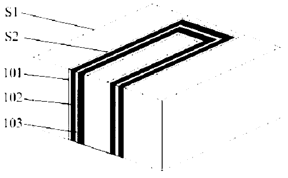
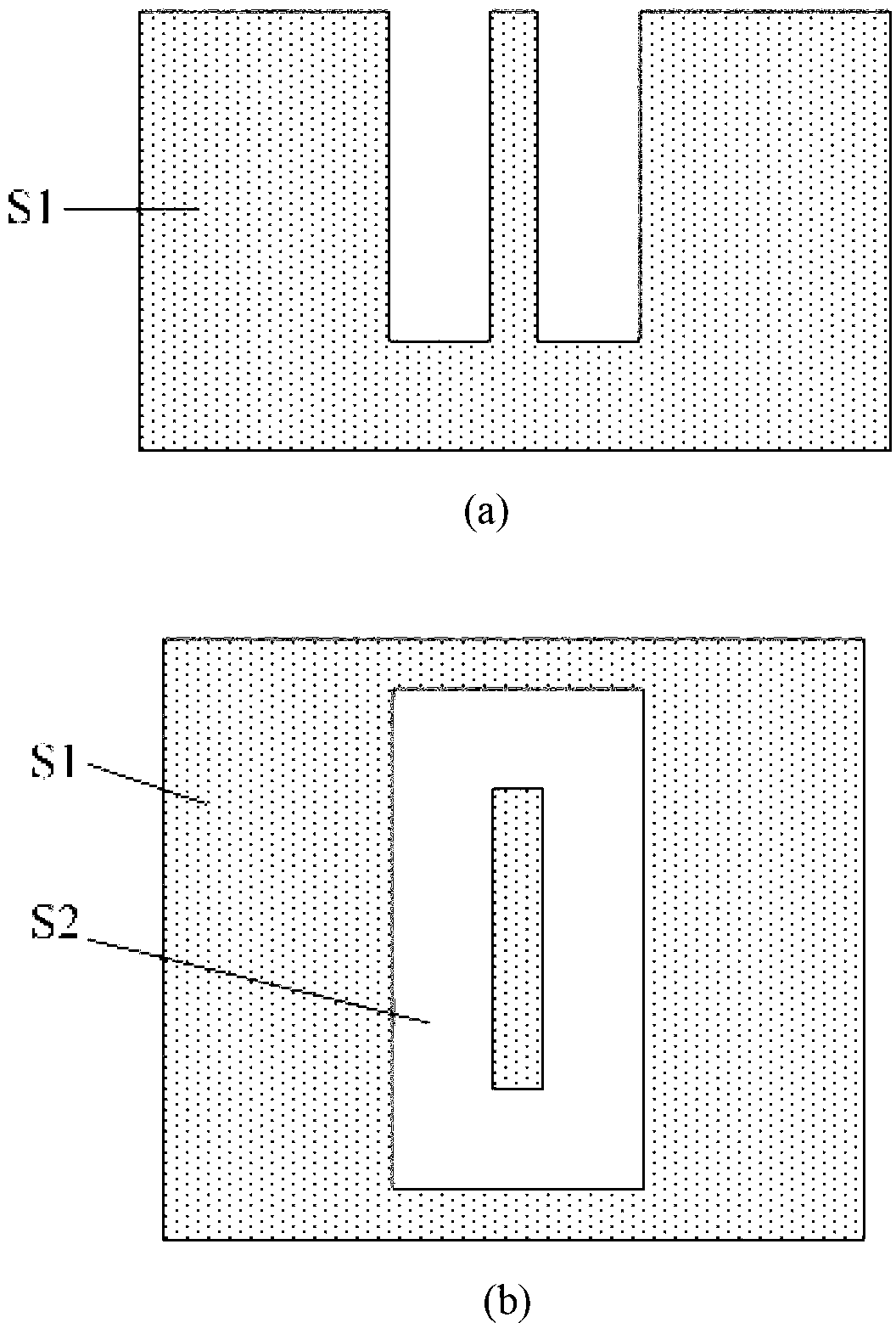
[0047] Such as figure 2 As shown, deep reactive ion etching technology is used to etch a circular deep groove S2 on the wafer substrate S1. The width of the deep trench is 5-10 microns; the length of the deep trench is not strictly limited, and can be 5-200 microns; the depth of the deep trench is less than the thickness of the wafer substrate, and can be 60-500 microns; the shape of the deep trench is One of a shape, a circular ring, or a polygonal ring.
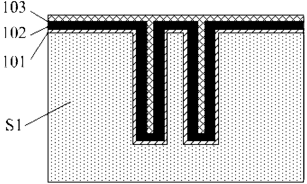
[0048] Such as image 3 As shown, the insulating layer 101 silicon dioxide is deposited on the inner wall of the deep trench by plasma enhanced chemical vapor deposition; the copper seed layer is deposited by sputtering technology, and the thickness of the copper layer is increased by electroplating to form a conductive layer 102. For inner and outer electrode plates. The thickness of the copper seed layer is not strictly...
specific Embodiment 2
[0051] Specific embodiment 2: vertical strip capacitor structure and manufacturing method thereof.
[0052] Such as Image 6 As shown, in this embodiment, the same manufacturing method as in Embodiment 1 is used to fabricate two strip-shaped deep groove structures S22 side by side. The production range of the length of the deep trench under the existing technology is 5-200 microns; the width of the deep trench in this embodiment is 3-5 microns; the depth of the deep trench is less than the thickness of the wafer substrate S21, which can be 60-500 microns; The distance between the deep grooves is 2-5 microns; the shape of the deep grooves is a rectangle or an "S" polygon.
[0053] Such as Figure 7 As shown, in this embodiment, the same manufacturing method as in Embodiment 1 is used to deposit the insulating layer 201 and deposit the conductive layer 202 in the deep trench S21 until the deep trench is filled.
[0054] Such as Figure 8 As shown, the silicon between the con...
specific Embodiment 3
[0057] Specific embodiment 3: vertical strip capacitor interdigitated parallel structure.
[0058] Such as Figure 11 As shown, this embodiment adopts the manufacturing method in Embodiment 2 to manufacture three vertical strip capacitors on the same wafer substrate, wherein 301 is an insulating layer, 302 is a conductive layer, and 303 is a dielectric layer, and then use The surface interconnection process forms the interdigitated electrodes S32 to form a parallel capacitor structure.
PUM
| Property | Measurement | Unit |
|---|---|---|
| width | aaaaa | aaaaa |
Abstract
Description
Claims
Application Information


