Display device
a display panel and display technology, applied in the field of display panels, can solve the problems of affecting the transmittance of the display panel, increasing the possibility of causing defects, etc., and achieve the effect of low power consumption
- Summary
- Abstract
- Description
- Claims
- Application Information
AI Technical Summary
Benefits of technology
Problems solved by technology
Method used
Image
Examples
embodiment 1
[0066]The following description will discuss Embodiment 1 of the present invention with reference to FIGS. 1 through 6.
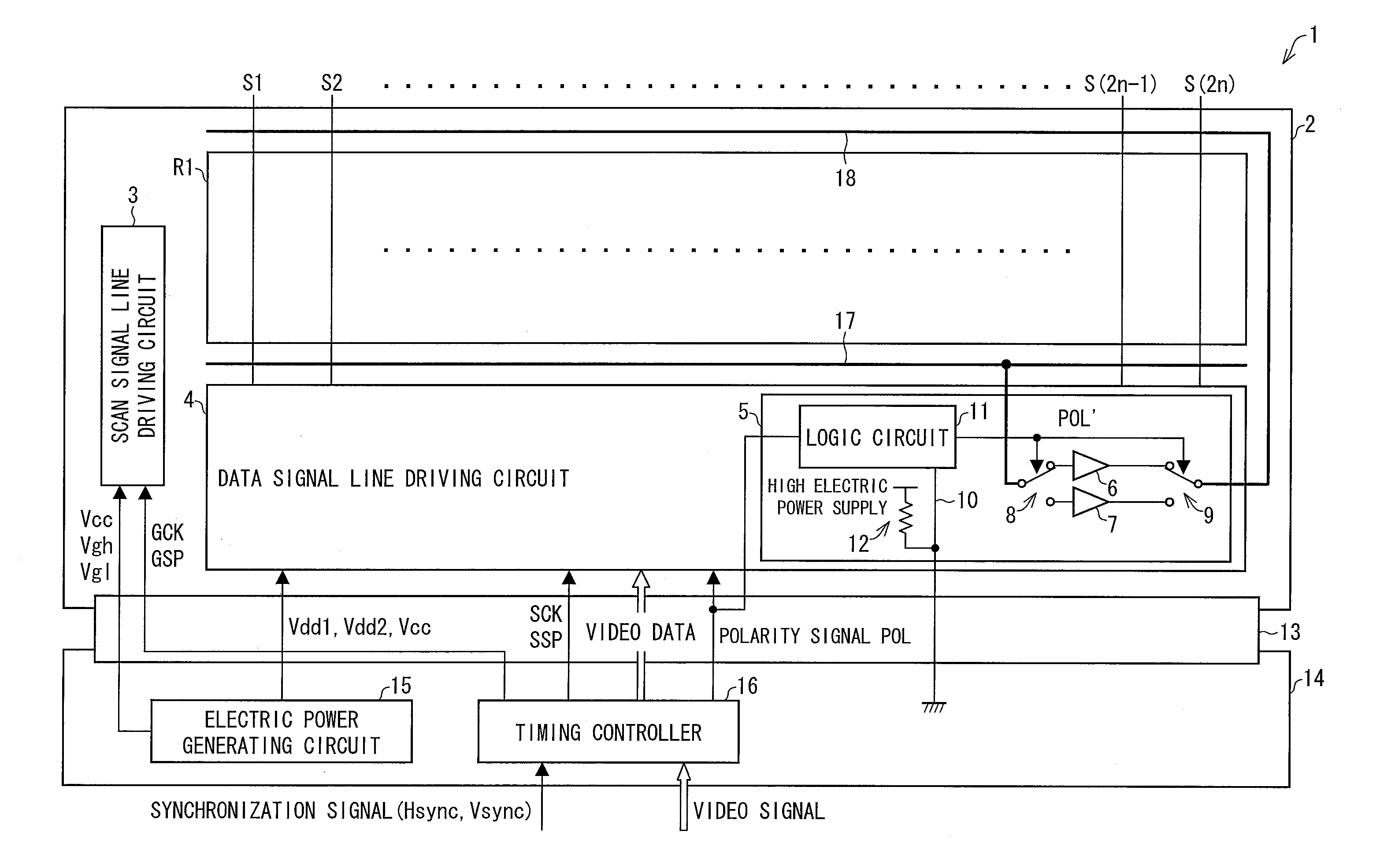
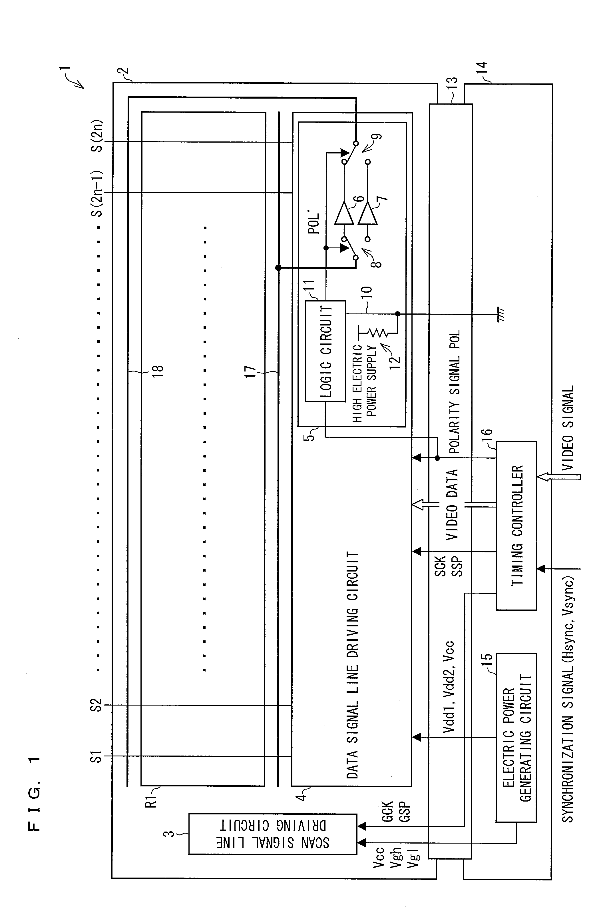
[0067]FIG. 1 is a view schematically illustrating a configuration of a liquid crystal display device 1.
[0068]The liquid crystal display device 1 includes (i) a liquid crystal display panel 2 and (ii) a control substrate 14 that is connected to the liquid crystal display panel 2 via an FPC 13 (see FIG. 1).
[0069]The liquid crystal display panel 2 has a display region R1 in which a plurality of pixels (not illustrated) are arranged in a matrix manner. The liquid crystal display panel 2 includes (i) a scan signal line driving circuit (gate driver) 3 for supplying scan signals to a plurality of scan signal lines (not illustrated) and (ii) a data signal line driving circuit (source driver) 4 for supplying data signals to a plurality of data signal lines S1, S2, . . . , and S(2n). The scan signal line driving circuit 3 and the data signal line driving circuit 4 are provide...
embodiment 2
[0113]The following description will discuss Embodiment 2 of the present invention with reference to FIGS. 7 through 9. Embodiment 2 is identical to Embodiment 1 except that a liquid crystal display device of Embodiment 2 includes (i) one (1) repair amplifier circuit 20 and one (1) repair amplifier circuit 21 each of which includes no polarity setting section 12, (ii) one (1) first auxiliary wire 17a and one (1) first auxiliary wire 17b and (iii) one (1) second auxiliary wire 18a and one (1) second auxiliary wire 18b.
[0114]FIG. 7 is a view schematically illustrating a configuration of a liquid crystal display panel 2a that includes the repair amplifier circuit 20 and the repair amplifier circuit 21 each of which includes no polarity setting section 12.
[0115]A polarity signal POL is supplied, via inverters 19, to pairs of switch sections 8 and 9 for the respective data signal lines S2, . . . , and S(2n) so as to have a polarity reverse to that of a polarity signal POL which is suppl...
embodiment 3
[0126]The following description will discuss Embodiment 3 of the present invention with reference to FIGS. 10 through 12. Embodiment 3 is identical to Embodiments 1 and 2 except that, in a liquid crystal display device of Embodiment 3, two of data signal lines S1, . . . , and S(2n), via which respective reverse data signals are supplied during one (1) horizontal period (1H period), are repaired by use of one (1) repair amplifier circuit 22 which includes one (1) positive-polarity amplifier circuit 6 and one (1) negative-polarity amplifier circuit 7.
[0127]FIG. 10 is a view schematically illustrating a configuration of a liquid crystal display panel 2b that includes the repair amplifier circuit 22.
[0128]The repair amplifier circuit 22 is electrically connected to one (1) first auxiliary wire 17c, one (1) first auxiliary wire 17d, one (1) second auxiliary wire 18c, and one (1) second auxiliary wire 18d (see FIG. 10).
[0129]For example, in a case where (i) dot reversal driving is employe...
PUM
 Abstract
Description
Claims
Application Information


