Housing-side separating layer for the stress decoupling of potted electronics

a technology of stress decoupling and separating layer, which is applied in the direction of electrical apparatus casings/cabinets/drawers, hermetically sealed casings, coatings, etc., can solve the problems of exacerbated problems, failure of the entire electrical circuit supported by the substrate, etc., to improve the adhesion of potting compound, improve the protection of the substrate against mechanical stresses, and free the interior surface.

Active Publication Date: 2014-01-30
CONTINENTAL TEVES AG & CO OHG
View PDF9 Cites 5 Cited by
  • Summary
  • Abstract
  • Description
  • Claims
  • Application Information

AI Technical Summary

Benefits of technology

[0022]In a particular development, the surface in the interior of the housing and / or of the substrate is plasma-cleaned in the process. With the aid of the plasmas, it is possible, in this case, to free the surface in the interior of the housing and / or of the substrate even more effectively from an extremely wide variety of materials, for example carbon compounds. This improves the adhesion of the potting compound in the housing and / or to the substrate and improves the protection of the substrate against mechanical stresses which are caused by movements of the potting compound.
[0023]In a further particular development, the surface in the interior of the housing and / or of the substrate is plasma-activated. In this case, activation is understood to mean an increase in the surface energy and / or surface tension. This increased surface energy further increases the adhesion of the potting compound to the surface in the interior of the housing and / or of the substrate.

Problems solved by technology

The problem is exacerbated in the event of changing mechanical loads, as can occur on account of thermal-expansion processes of the potting compound in the event of fluctuations in temperature.
Finally, the tensile load which acts on the electronic components may be responsible for cracks in the electrical contact-making points, these cracks leading to failure of the entire electrical circuit which is supported by the substrate.

Method used


Image

  • Housing-side separating layer for the stress decoupling of potted electronics
  • Housing-side separating layer for the stress decoupling of potted electronics

Examples


Embodiment Construction

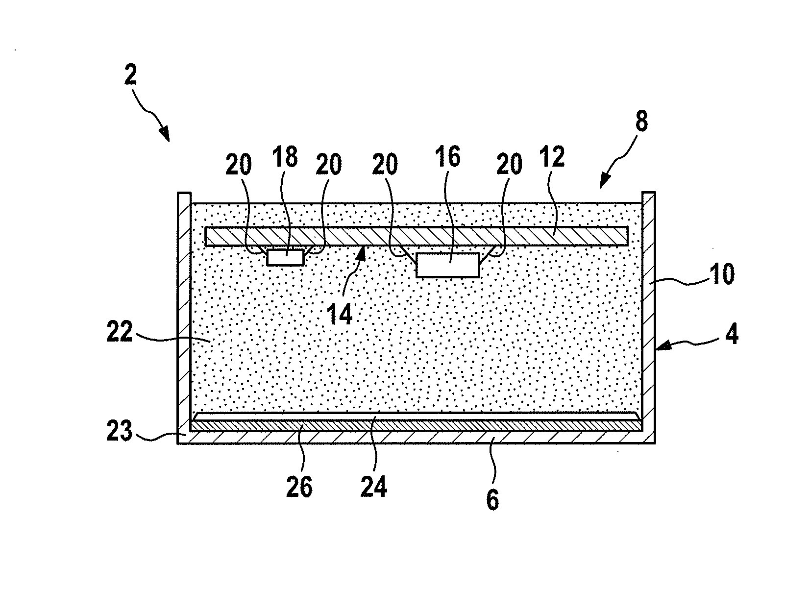
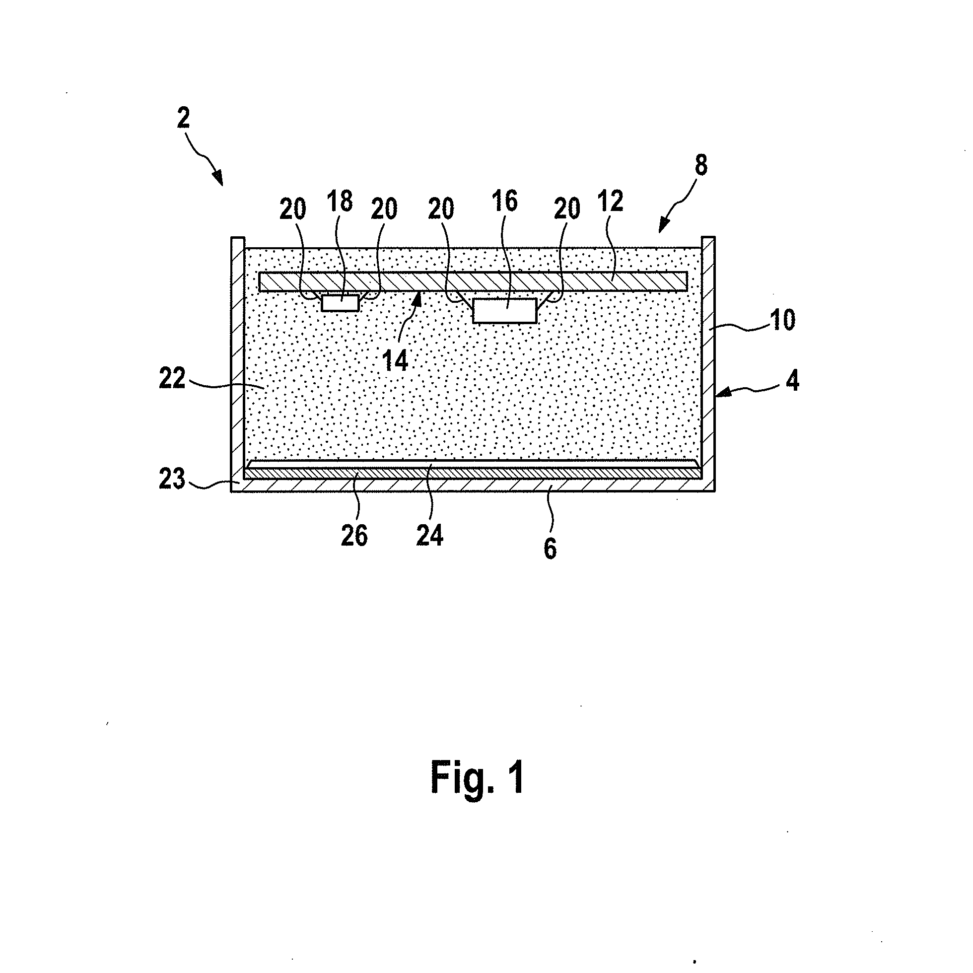
[0028]Reference is made to FIG. 1 which shows a schematic illustration of an exemplary apparatus 2 according to the invention.

[0029]The apparatus 2 has a housing 4 which a housing base 6, a housing opening 8 which is situated opposite the housing base 6, and a housing casing 10 which connects the housing base 6 and the housing opening 8.

[0030]A substrate 12, which supports an electrical circuit 14 on its side which is directed toward the housing base 6, is enclosed in the housing 4. A first electronic component 16 and a second electronic component 18, which each comprise two electrical contacts 20 to conductor tracks (not shown) of the electronics circuit 14, of the circuit 14 are indicated in FIG. 1. In this case, the substrate 12 can be a printed circuit board which is composed of a thermoplastic, duroplastic or polyimide, or can be a ceramic support.

[0031]The electrical circuit 14 is surrounded by a potting compound 22 in the housing 4. The potting compound adheres to the wall 23...


PUM


Abstract

The invention relates to a device, which includes a substrate for carrying an electrical circuit, a housing for enclosing the substrate, and a potting compound accommodated in the housing, which potting compound at least partially encloses the substrate. The potting compound can adhere to the housing. Furthermore, the device has a wall, from which the potting compound can detach.

Description

CROSS REFERENCE TO RELATED APPLICATIONS[0001]This application is the U.S. National Phase Application of PCT / EP2012 / 056139, filed Apr. 4, 2012, which claims benefit of German Patent Application Nos. 10 2011 007 012.5, filed Apr. 7, 2011 and 10 2011 086 048.7, filed Nov. 9, 2011, the contents of such applications being incorporated by reference herein.FIELD OF THE INVENTION[0002]The present invention relates to an apparatus comprising a substrate for supporting an electrical circuit, a housing for enclosing the substrate, and a potting compound which is accommodated in the housing and at least partially surrounds the substrate, and to a method for producing an apparatus of this kind.BACKGROUND OF THE INVENTION[0003]The potting compound protects the substrate in the housing against environmental influences. The potting compound could also mechanically fix the printed circuit board in the housing.[0004]In this case, the substrate can be completely surrounded by the potting compound.SUMM...

Claims


Application Information

Patent Timeline
Patent Type & Authority Applications(United States)
IPC IPC(8): H05K7/14H05K5/06
CPCH05K5/064H05K7/14H05K5/0056H05K5/00H05K5/06
Inventor SCHILLINGER, JAKOBHUBER, DIETMARTHEOBALD, DIRK
Owner CONTINENTAL TEVES AG & CO OHG
Why Eureka
Try Eureka