Semiconductor Package Having Buss-Less Substrate

a technology of semiconductors and substrates, applied in resist details, non-metallic protective coating applications, patterning and lithography, etc., can solve the problems of limiting the number of signal traces in advanced bga devices, unable to place signal traces, and low so as to avoid plating the sidewall of the trace, keep the electrical resistance and trace fatigue low, and enhance the adhesion to plastic encapsulation compounds

Active Publication Date: 2009-02-26
TEXAS INSTR INC
View PDF8 Cites 31 Cited by
  • Summary
  • Abstract
  • Description
  • Claims
  • Application Information

AI Technical Summary

Benefits of technology

[0014]It is a technical advantage of the using a seed layer for distributing the electrical plating potential that buss or tie bars are no longer required and the substrate design space thus gained can be used for additional signal traces. In addition, the electroplating process is well suited for creating traces of specific aspect ratios to keep electrical resistance and trace fatigue low, while enhancing the adhesion to plastic encapsulation compounds of the oxidized copper trace sidewalls. The electroplating process is also well suited to deposit thin nickel layers.
[0015]In is another technical advantage that the plating the trace sidewalls is avoided. Not only does this avoidance save precious metal (such as gold or palladium), it also gains about 1.5 μm in trace spacing and thus supports denser layout of the traces. Consequently, the process of the invention represents a universal solution for thin nickel / gold layers.

Problems solved by technology

As a popular plating technique, electroplating offers controls for thick as well as thin layers, while electroless plating is not generally suitable for thin nickel layers (less than 0.5 μm).
Bus and tie bars consume precious substrate real estate, which thus cannot be available for placing signal traces.
Consequently, the need for bus and tie bars limits the number of signal traces in advanced BGA devices.
Consequently, the need for bus and tie bars introduces a reliability hazard for the finished BGA devices.
Consequently, the fine substrate pitches required for advanced BGA high signal devices are difficult to achieve.
In addition, while copper surfaces, which oxidize easily, are favorable for strong adhesion to epoxy-based molding compounds, nickel and noble metals degrade the adhesion.
Further, the generous plating of traces with precious metals is actually wasteful and expensive.
These layers, however, have to be patterned into traces, and the traces of the various layers have to be interconnected with metal-filled through-holes (so-called conductive vias)—an altogether expensive solution, considering the fact that each additional metal layer and the required vias add between 10% and 30% to the substrate cost.

Method used


Image

  • Semiconductor Package Having Buss-Less Substrate
  • Semiconductor Package Having Buss-Less Substrate
  • Semiconductor Package Having Buss-Less Substrate

Examples


Embodiment Construction

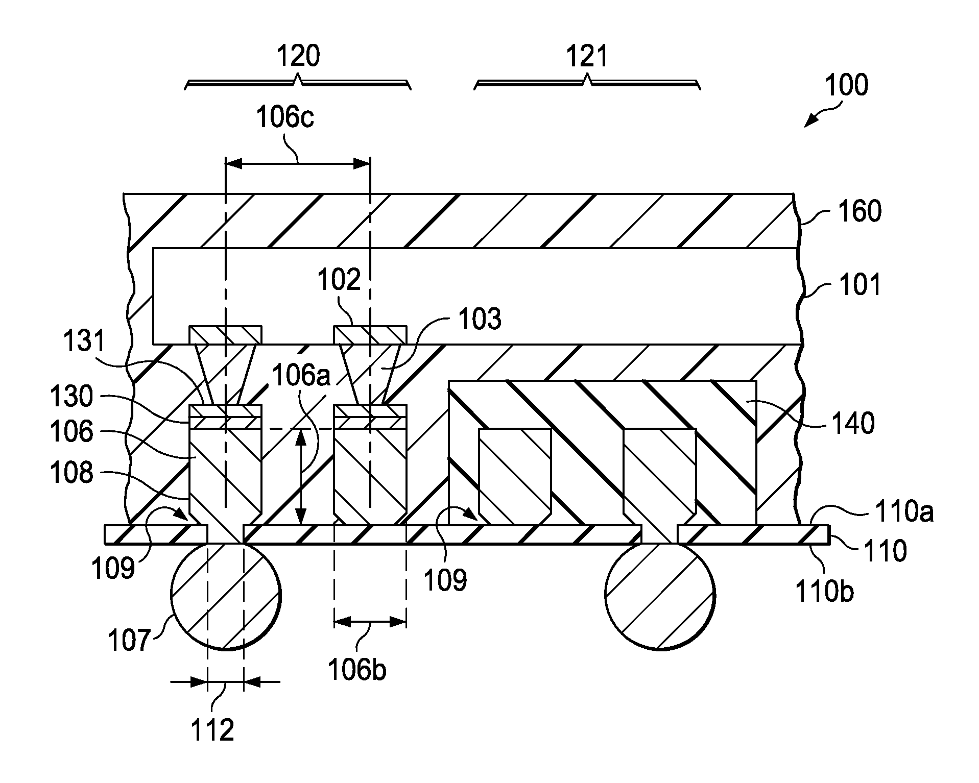
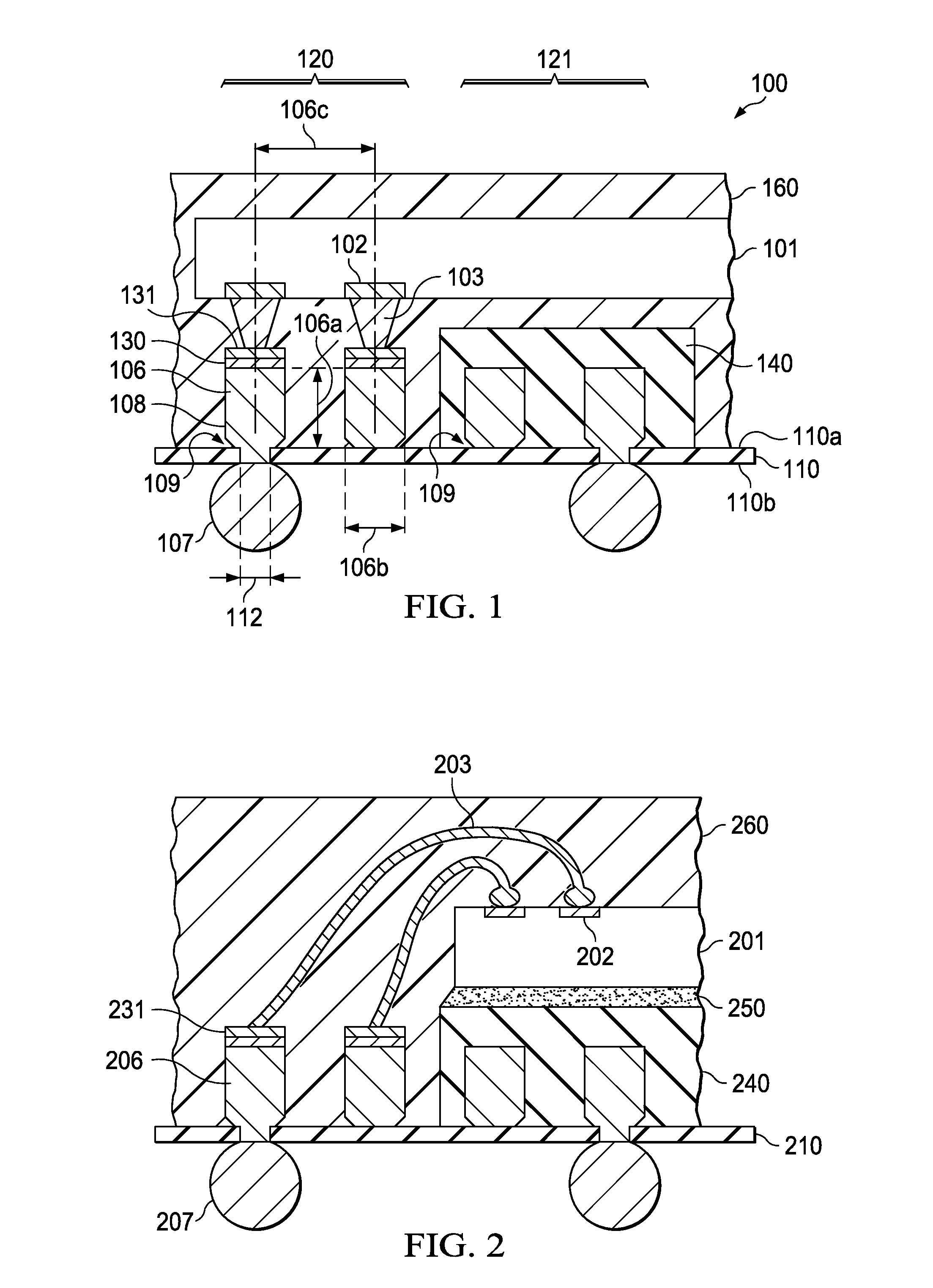
[0034]FIGS. 1 and 2 illustrate cross sections of portions of exemplary BGA devices, which include embodiments of the invention. In FIG. 1, the device, generally designated 100, has chip 101 with terminals 102, onto which metallic studs 103 are affixed as chip contacts. Studs 103 are preferably made of gold; alternatively, studs 103 may be made of copper or a copper alloy. While studs 103 are schematically depicted as a truncated cones, their actual shapes may be more complex.

[0035]FIG. 1 depicts a portion of the substrate, onto which chip 101 is assembled. The substrate includes the insulating tape 110 with first surface 110a and second surface 110b. Insulating tape 110 is preferably a sheet of a polyimide compound with a thickness ranging from about 40 to 80 μm. The through-holes with diameter 112 extend through the substrate base from the first surface 110a to the second surface 110b. Through-hole diameter 112 is preferably in the range from 50 to 120 μm. As FIG. 1 shows, the thro...


PUM

PropertyMeasurementUnit
thicknessaaaaaaaaaa
thicknessaaaaaaaaaa
thicknessaaaaaaaaaa

Abstract

A ball grid array device with an insulating substrate (110) having metal traces (106, for example copper, about 18 μm thick) with sidewalls (108) at right angles to the trace top. The traces are grouped in a first (120) and a second set (121). The first set traces have the top surface covered by a thin noble metal (for example a nickel layer (130) about 0.1 μm thick and an outermost gold layer (131) about 0.5 μm thick), while the sidewalls are un-covered by the noble metal. About 1.5 μm are thus gained for the trace spacing; oxidation of the trace sidewalls is enabled. The second set traces have the top surface un-covered by the noble metal; the traces are covered by an insulating soldermask. A semiconductor chip (101) with terminals (102) is attached to the substrate with the terminals connected to the noble metal of the first set traces, either by bonding wires (for example gold) or by metal studs (for example gold). The assembled chip and the first set traces are encapsulated in a polymerized compound (160), which adheres to the oxidized trace sidewalls and locks into the trace undercuts at the substrate interface.

Description

FIELD OF THE INVENTION[0001]The present invention is related in general to the field of semiconductor devices and processes, and more specifically to the structure and fabrication process of substrates of ball grid array packages combining small size with high signal numbers.DESCRIPTION OF RELATED ART[0002]In the popular ball-grid-array (BGA) packages of electronic devices, the semiconductor chip is inside the package, assembled on an insulating substrate with at least one metal layer for interconnecting traces. On the outside of the substrate are the solder balls for connection to external parts.[0003]In recent years, the flip-mounting of the chips onto the substrates has become the favorite assembly technique for BGA packages, because flip-chip assembly offers the thinnest packages and thus supports the ongoing trend of device miniaturization. The semiconductor chips, which are intended for the flip-operation, have their terminals prepared with metal bumps, such as gold studs or s...

Claims


Application Information

Patent Timeline
Patent Type & Authority Applications(United States)
IPC IPC(8): H01L23/488
CPCH01L23/498H01L23/49816H01L24/83H01L2924/01033H05K2203/0574H05K3/426H05K3/28H05K3/243H01L24/45H01L24/48H01L24/81H01L2224/13144H01L2224/13147H01L2224/16H01L2224/45144H01L2224/48091H01L2224/48465H01L2224/48599H01L2224/73265H01L2224/81801H01L2224/8385H01L2924/01013H01L2924/01014H01L2924/01028H01L2924/01029H01L2924/01031H01L2924/01032H01L2924/01046H01L2924/01061H01L2924/01078H01L2924/01079H01L2924/014H01L2924/14H01L2924/15311H01L2924/3025H05K1/0393H05K3/062H05K3/108H01L2924/00014H01L2924/00H01L2224/05571H01L2224/05573H01L2924/181H01L2924/00012H01L2224/05599
Inventor ABBOTT, DONALD C.
Owner TEXAS INSTR INC
Why Eureka
Try Eureka