

Semiconductor device
a technology of semiconductors and devices, applied in the direction of semiconductor devices, electrical devices, transistors, etc., can solve the problems of reducing on-resistance and switching characteristics, and it is difficult to realize comparable blocking breakdown voltage in the forward and reverse direction
- Summary
- Abstract
- Description
- Claims
- Application Information
AI Technical Summary
Benefits of technology
Problems solved by technology
Method used
Image

Examples
first embodiment
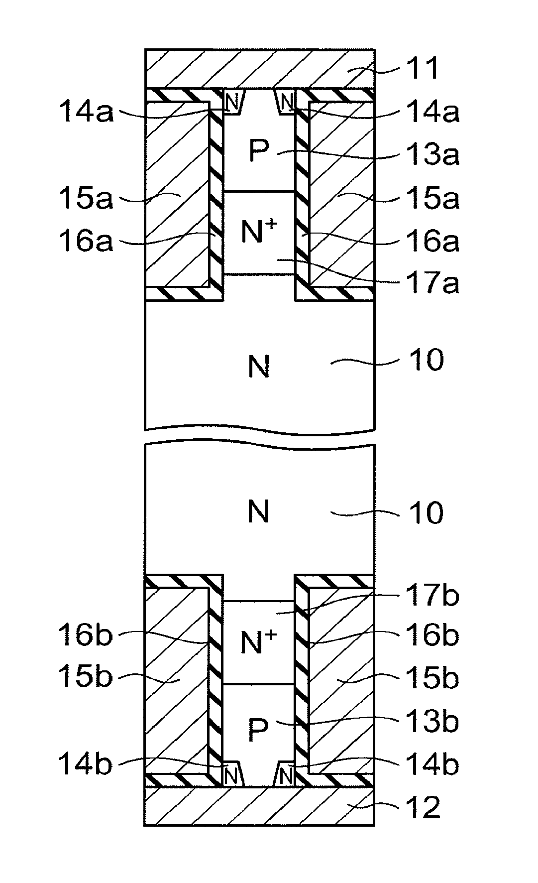
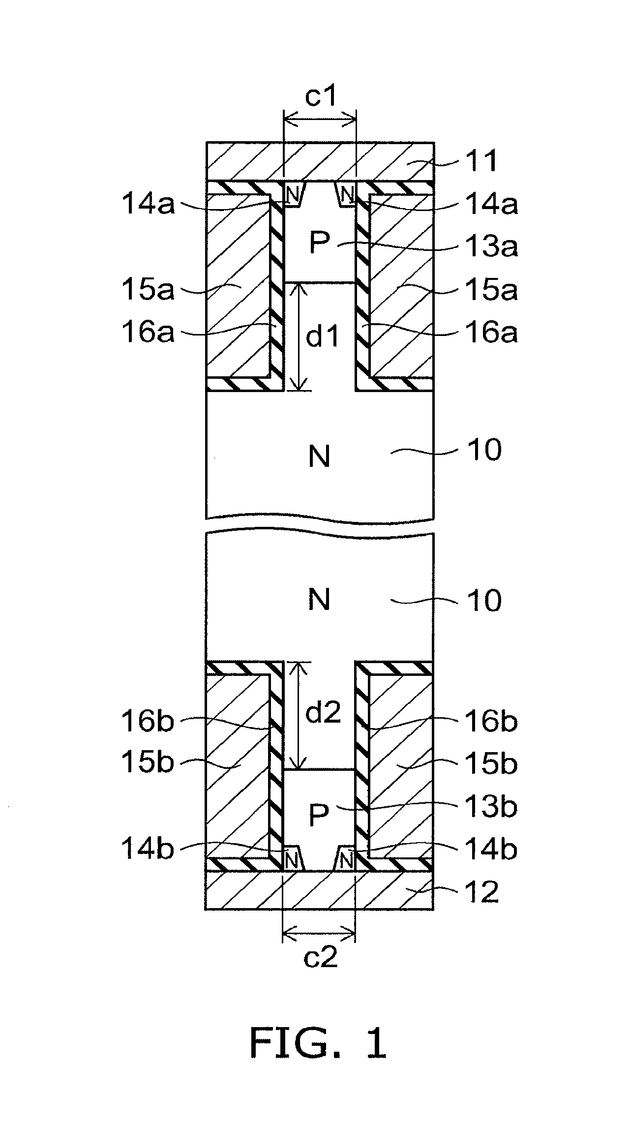
[0026]FIG. 1 is a schematic cross-sectional view of a relevant part of a semiconductor device according to a first embodiment of the invention.
[0027]The semiconductor device according to this embodiment is a vertical device in which a current path is formed in the vertical direction connecting between a first main electrode 11 and a second main electrode 12 provided on the front and rear surface, respectively, of a semiconductor layer. The semiconductor device according to this embodiment includes a cell section in which the current path is formed and a terminal section formed outside the cell section so as to surround the cell section. In FIG. 1, part of the cell section is shown. The structure shown in FIG. 1 is repeated laterally. Also in other embodiments, only the cell section is shown and described.
[0028]The semiconductor device according to this embodiment includes an N-type base layer 10, a first P-type base layer 13a provided on the first major surface side of the N-type ba...
second embodiment
[0057]FIG. 4 is a schematic cross-sectional view of a relevant part of a semiconductor device according to a second embodiment of the invention.
[0058]In this embodiment, in addition to the configuration of the above first embodiment, an N+-type first stopper layer 17a having a higher N-type impurity concentration than the N-type base layer 10 is provided in the portion of the N-type base layer 10 in contact with the first P-type base layer 13a, and an N+-type second stopper layer 17b having a higher N-type impurity concentration than the N-type base layer 10 is provided in the portion of the N-type base layer 10 in contact with the second P-type base layer 13b.
[0059]The second stopper layer 17b can suppress the depletion layer from extending to the second P-type base layer 13b during application of forward voltage, and the first stopper layer 17a can suppress the depletion layer from extending to the first P-type base layer 13a during application of reverse voltage. Thus, the effec...
third embodiment
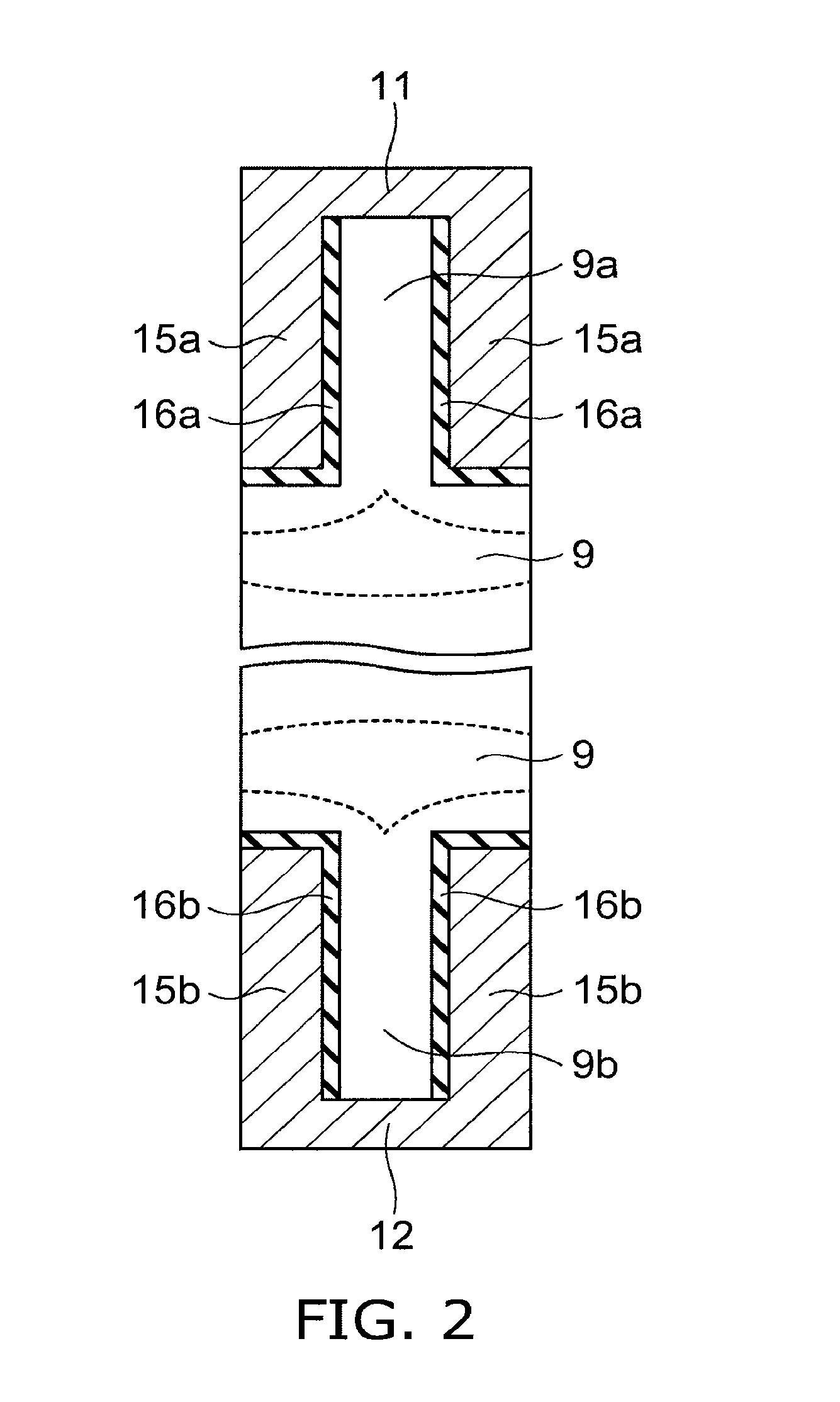
[0061]FIG. 5 is a schematic cross-sectional view of a relevant part of a semiconductor device according to a third embodiment of the invention.
[0062]In this embodiment, in addition to the configuration of the above second embodiment, a third P-type base layer 18 is provided adjacent to the N-type base layer 10. The third P-type base layer 18 is adjacent in the lateral direction, which is generally parallel to the first major surface and the second major surface of the N-type base layer 10. The N-type base layer 10 is provided in the portion vertically connecting between the first P-type base layer 13a and the second P-type base layer 13b, and the third P-type base layer 18 is provided in the portion vertically connecting between the first gate electrode 15a and the second gate electrode 15b.
[0063]The N-type base layers 10 and the third P-type base layers 18 are adjacent (form a pn junction) alternately in the lateral direction and periodically arranged to constitute a so-called “su...
PUM
 Abstract
Description
Claims
Application Information