Photoelectric device

a photoelectric device and photoelectric technology, applied in the direction of semiconductor devices, basic electric elements, electrical equipment, etc., can solve the problem that the cost of power generation from industrial solar cells remains higher than that of fossil fuel power generation, and achieve the effects of reducing optical loss, reducing recombination loss of carriers, and simplifying manufacturing processes

Inactive Publication Date: 2014-02-06
INTELLECTUAL KEYSTONE TECH LLC
View PDF7 Cites 15 Cited by
  • Summary
  • Abstract
  • Description
  • Claims
  • Application Information

AI Technical Summary

Benefits of technology

[0007]One or more embodiments of the present invention provide for photoelectric devices that can reduce optical loss, reduce recombination loss of carriers, and have a simplified manufacturing process. Additional aspects will be set forth in part in the description that follows and, in part, will be apparent from the description, or may be learned by practice of the presented embodiments.

Problems solved by technology

However, the cost of power generation from an industrial solar cell remains higher than that of fossil fuel power generation.

Method used


Image

  • Photoelectric device
  • Photoelectric device
  • Photoelectric device

Examples


Embodiment Construction

[0034]The present invention will now be described more fully with reference to the accompanying drawings, in which exemplary embodiments of the invention are shown.

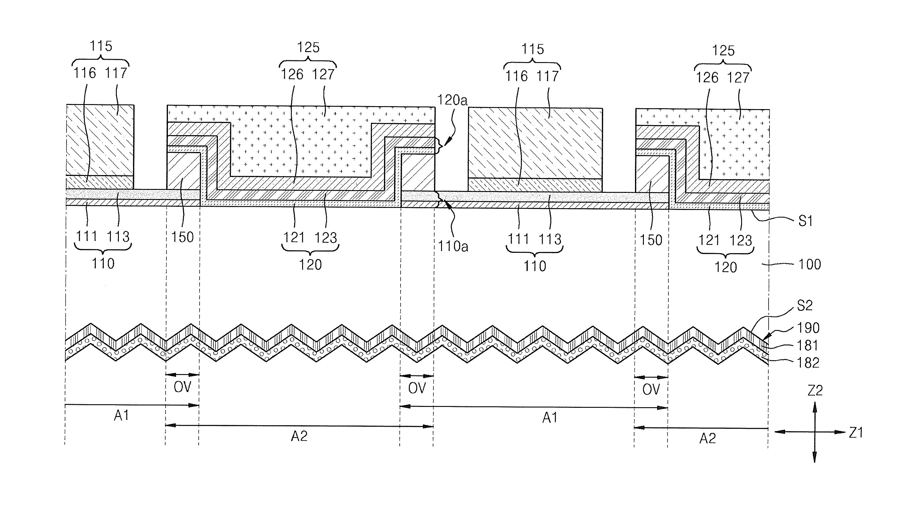
[0035]FIG. 1 is a cross-sectional view of a photoelectric device according to an embodiment of the present invention.

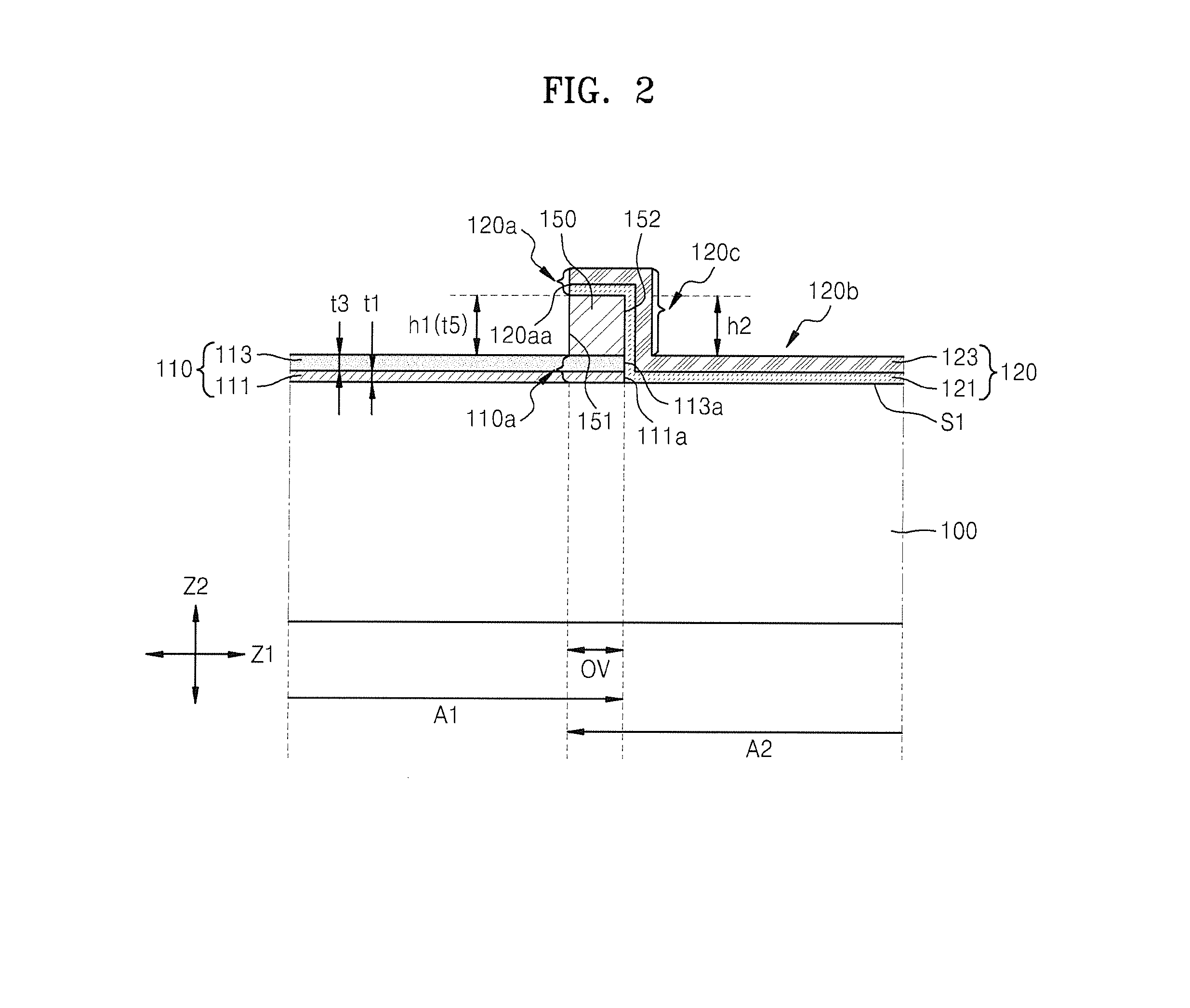
[0036]Referring to FIG. 1, the photoelectric device includes a semiconductor substrate 100, a first conductive type (for example, n-type) first semiconductor stack 110 and a second conductive type (for example, p-type) second semiconductor stack 120, which are formed on the semiconductor substrate 100, and first and second electrodes 115 and 125 electrically connected to the first and second semiconductor stacks 110 and 120. For example, a plurality of the first and second semiconductor stacks 110 and 120 may be formed and alternately arranged on the semiconductor substrate 100.

[0037]The semiconductor substrate 100 has a first surface S1 and a second surface S2 opposite to the first surface S1. A base elect...


PUM


Abstract

A photoelectric device that reduces optical loss, reduces recombination loss of carriers, and can be manufactured by using a simplified process is provided. The photoelectric device includes a semiconductor substrate, a first semiconductor stack on a first surface of the semiconductor substrate and having a first conductivity, and a second semiconductor stack on the first surface of the semiconductor substrate and having a second conductivity opposite to the first conductivity. Edge portions of the first and second semiconductor stacks face each other with an insulating portion therebetween.

Description

CROSS-REFERENCE TO RELATED APPLICATION[0001]This application claims priority to and the benefit of Korean Patent Application No. 10-2012-0084986, filed on Aug. 2, 2012 in the Korean Intellectual Property Office, the entire content of which is incorporated herein by reference.BACKGROUND[0002]1. Field[0003]Aspects of embodiments of the present invention relate to photoelectric devices.[0004]2. Description of the Related Art[0005]Recently, due to the increased demand for finite energy sources (such as fossil fuels) and to the worsening global environmental problems, the development of clean energy has accelerated. As a clean energy, solar power generation that uses solar energy is expected to be a widely used energy source since solar energy may be directly converted to electricity.[0006]However, the cost of power generation from an industrial solar cell remains higher than that of fossil fuel power generation. An increase in efficiency of the solar power generation would allow more wi...

Claims


Application Information

Patent Timeline
Patent Type & Authority Applications(United States)
IPC IPC(8): H01L31/076
CPCH01L31/076H01L31/022441H01L31/03529H01L31/0682H01L31/0747Y02E10/547Y02E10/548H01L31/042
Inventor LEE, CHO-YOUNGOH, MIN-SEOKSONG, NAM-KYUKIM, YU-KYUNGLEE, YUN-SEOK
Owner INTELLECTUAL KEYSTONE TECH LLC
Why Eureka
Try Eureka