Semiconductor package having an antenna and manufacturing method thereof

a technology of semiconductor devices and semiconductors, applied in the field of semiconductor devices with antennas, can solve the problems of high manufacturing cost, difficult to achieve compact product design, and difficult to reduce device siz

Active Publication Date: 2014-02-06
ADVANCED SEMICON ENG INC
View PDF2 Cites 77 Cited by
  • Summary
  • Abstract
  • Description
  • Claims
  • Application Information

AI Technical Summary

Benefits of technology

[0005]One aspect of the disclosure relates to a semiconductor package. In one embodiment, the semiconductor package includes a first substrate including a ground layer; an interposer disposed on an upper surface of the first substrate and having at least one opening; a first die disposed in the at least one opening and coupled to the first substrate; a second substrate coupled to the interposer, disposed over the first substrate and having an area less than an area of the first substrate; a second die disposed on a lower surface of the second substrate; a third die embedded within the second substrate; an inductor disposed on an upper surface of the second substrate wherein the inductor is electrically connected to the second die and the third die; a package body encapsulating portions of the first substrate, the interposer, the second substrate, the first die and the second die, the package body having a lateral surface and an upper surface; an

Problems solved by technology

Accordingly, higher manufacturing costs are incurred and a compact pr

Method used


Image

  • Semiconductor package having an antenna and manufacturing method thereof
  • Semiconductor package having an antenna and manufacturing method thereof
  • Semiconductor package having an antenna and manufacturing method thereof

Examples


Embodiment Construction

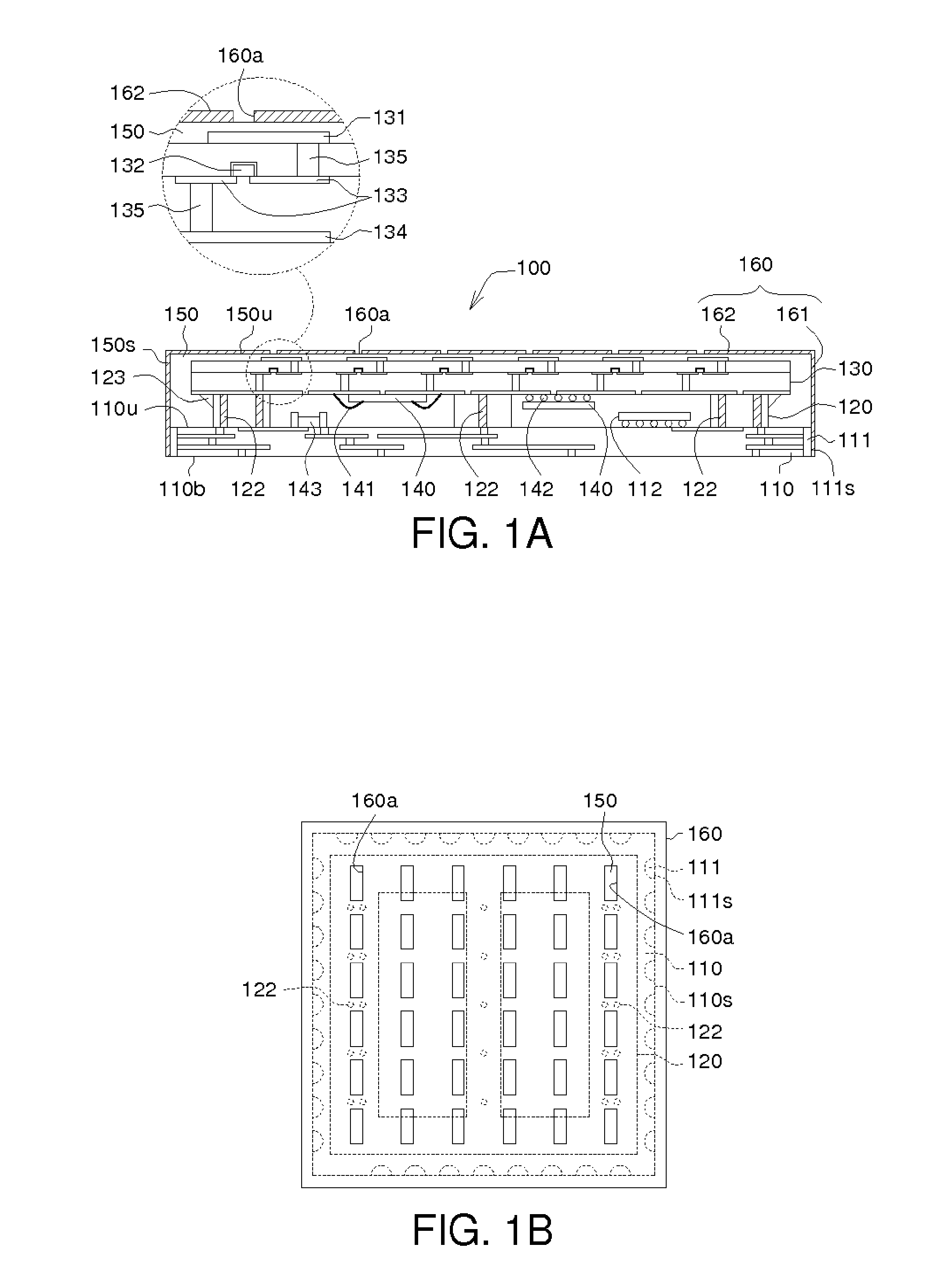
[0024]Referring to FIG. 1A, a cross-sectional view of a semiconductor package 100, according to one embodiment of the invention, is illustrated. The semiconductor package 100 includes a first substrate 110, an interposer substrate 120, a second substrate 130, a plurality of semiconductor chips 140, a package body 150 and a first antenna layer 160.

[0025]The first substrate 110 has an upper surface 110u and a lower surface 110b opposite to the upper surface 110u, and includes a grounding segment 111. The first substrate 110 can be a multi-layered organic substrate or a ceramic substrate, for example. In addition, at least a semiconductor chip 112 and a passive component 143 are further disposed on the upper surface 110u of the first substrate 110 and electrically connected to the first substrate 110. For example, the semiconductor chip 112 disposed on the first substrate 110 may include a baseband chip.

[0026]In the present embodiment, the grounding segment 111 is a conductive pillar w...


PUM


Abstract

A semiconductor package and a manufacturing method thereof are provided. The semiconductor package includes a first substrate, a second substrate, an interposer substrate, a semiconductor chip, a package body and a first antenna layer. The first substrate comprises a grounding segment. The interposer substrate is disposed between the second substrate and the first substrate. The semiconductor chip is disposed on the second substrate. The package body encapsulates the second substrate, the semiconductor chip and the interposer substrate, and has a lateral surface and an upper surface. The first antenna layer is formed on the lateral surface and the upper surface of the package body, and electrically connected to the grounding segment.

Description

BACKGROUND OF THE INVENTION[0001]1. Field of the Invention[0002]The invention relates in general to a semiconductor package and a manufacturing method thereof, and more particularly to a semiconductor package with an antenna and a manufacturing method thereof.[0003]2. Description of the Related Art[0004]Wireless communication devices, such as cell phones, require antennas for transmitting and receiving radio frequency (RF) signals. Conventionally, a wireless communication device includes therein an antenna and a communication module (e.g., a semiconductor package with RF communication capability), each disposed on different parts of a circuit board. Under the conventional approach, the antenna and the communication module are separately manufactured and electrically connected after being placed on the circuit board. Accordingly, higher manufacturing costs are incurred and a compact product design as well as reduced device size are difficult to achieve. In addition, a RF signal trans...

Claims


Application Information

Patent Timeline
IPC IPC(8): H01L29/86H01L21/78
CPCH01L23/295H01L23/3135H01L21/568H01L23/66H01L24/16H01L24/48H01L24/97H01L2223/6627H01L2223/6677H01L2224/16225H01L2224/48227H01L2224/97H01L2924/15192H01L2924/15311H01L2924/19041H01L2924/19042H01L2924/19043H01L2924/19105H01Q21/0087H01Q21/064H01Q21/065H01L2924/3011H01L2924/3025H01L2924/15787H01L2924/12042H01L2924/00014H01L2924/181H01L23/552H01L2224/81H01L2224/85H01L2924/00H01L2224/45099H01L2224/45015H01L2924/207
Inventor LIN, I-CHIAJOU, SHENG-JIANYEN, HAN-CHEE
Owner ADVANCED SEMICON ENG INC
Why Eureka
Try Eureka