Probe card with simplified registration steps and manufacturing method thereof

a technology of registration steps and manufacturing methods, applied in the field of probe cards, can solve the problems of affecting the efficiency of inspection, the inability of inspectors to observe directly and determine, and the relative long registration time, so as to speed up the registration procedure greatly and facilitate the subsequent test steps

Inactive Publication Date: 2014-02-06
HUANG JUNG TANG
View PDF0 Cites 6 Cited by
  • Summary
  • Abstract
  • Description
  • Claims
  • Application Information

AI Technical Summary

Benefits of technology

[0013]In conclusion, as regards a probe card put forth by the present invention, the first carrier board is at least partially light-transmitted. Hence, to perform the procedure of registration between the probe card and a device under test (DUT), it is feasible for an inspector to watch from above the probe card directly the relative position between the probe card and the DUT, an

Problems solved by technology

The aforesaid process requires comparing repeatedly the pictures taken of the DUT and the probe card and thus results in relatively long registration time.
Also, if the probes do not actually come into contact with the pads or the pro

Method used


Image

  • Probe card with simplified registration steps and manufacturing method thereof
  • Probe card with simplified registration steps and manufacturing method thereof
  • Probe card with simplified registration steps and manufacturing method thereof

Examples


first embodiment

[0022]To overcome the drawbacks of the prior art, the present invention puts forth a probe card and a probe card manufacturing method. The structures and benefits of the probe card according to the first embodiment of the present invention are described below.

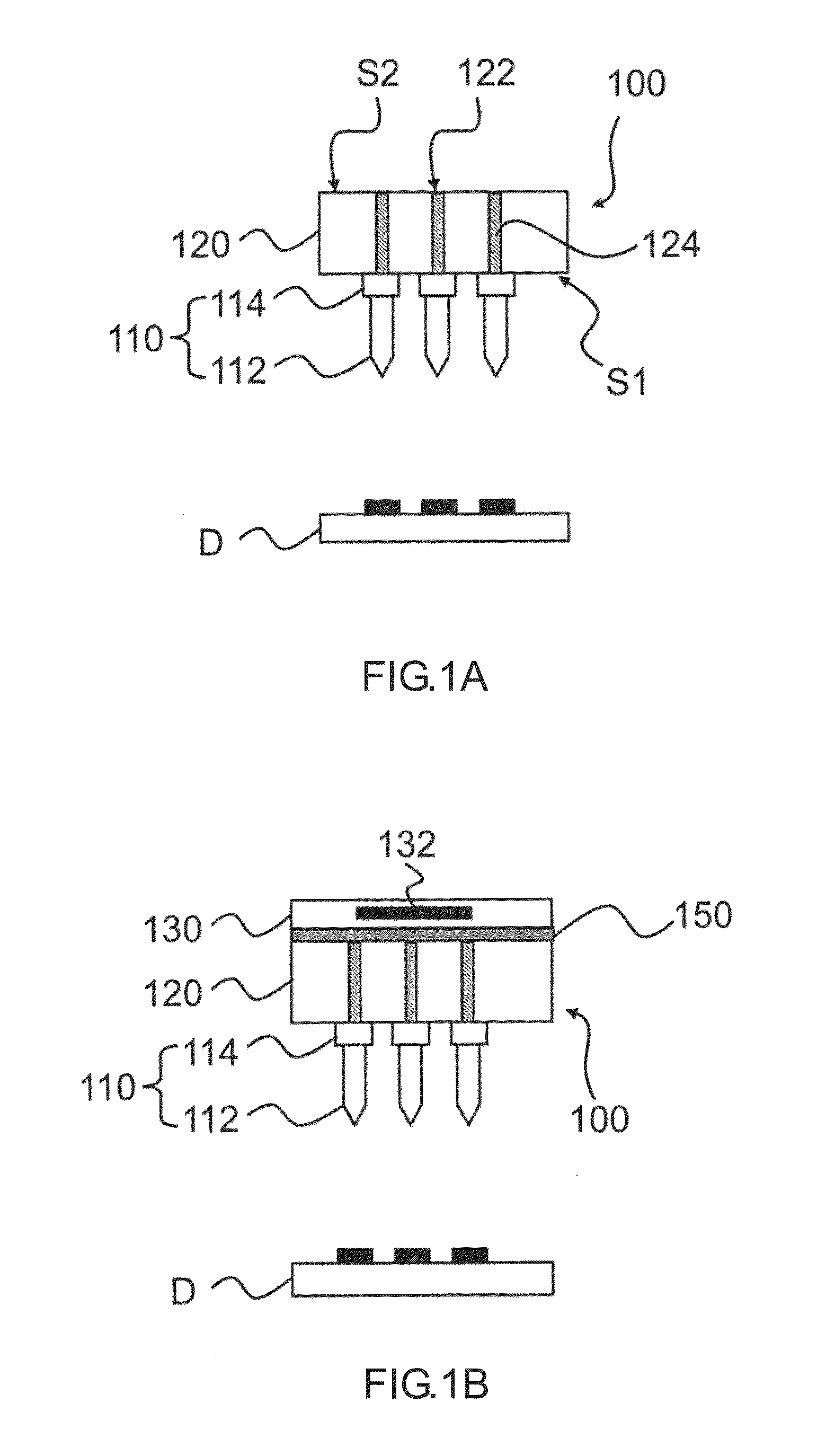
[0023]FIG. 1A, there is shown a structural schematic view of a probe card according to the first embodiment of the present invention. Referring to FIG. 1A, a probe card 100 in this embodiment comprises a probe module 110 and a first carrier board 120. The probe module 110 is disposed on the first carrier board 120 and has a plurality of probes 112. The first carrier board 120 is at least partially light-transmitted.

[0024]As regards the probe card 100 in this embodiment, the first carrier board 120 has a first surface S1 and a second surface S2 opposing the first surface S1. The probe module 110 is disposed on the first surface S1 of the first carrier board 120 and comprises the plurality of probes 112 and a plurality of bumps 1...

second embodiment

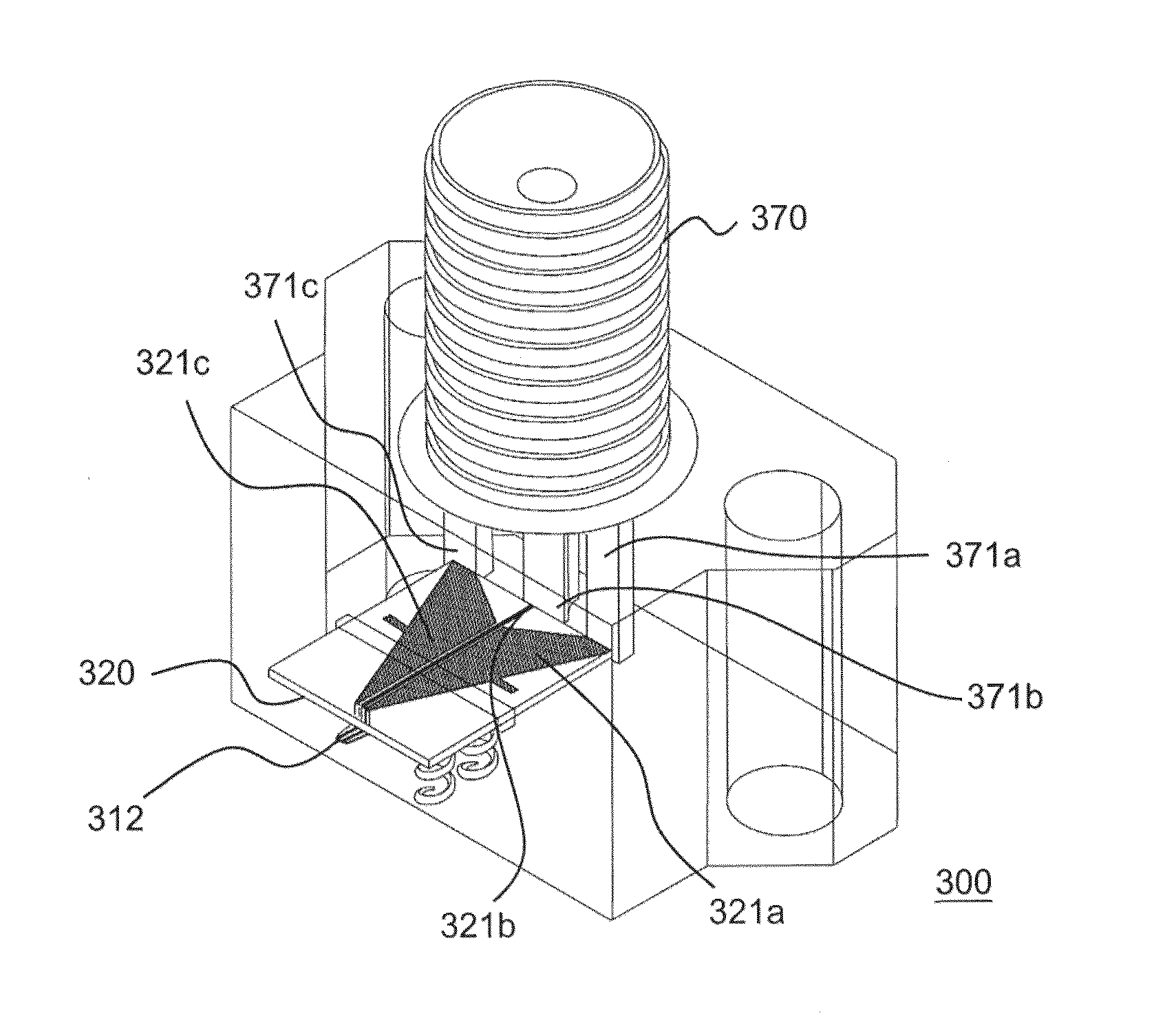
[0039]Although the present invention is characterized in that the probes 112 of the probe card 100 are perpendicular to the first carrier board 120, the present invention is not restricted to the aforesaid technical feature. FIG. 4A through FIG. 4E are structural schematic views of the probe card according to the second embodiment of the present invention. FIG. 4A is a top view of the probe card. FIG. 4B is a top view of the probe card having a circuit module thereon. FIG. 4C is a right perspective view of FIG. 4B. As regards a probe card 300 of FIG. 4A, a plurality of probes 312 is parallel to the surface of a first carrier board 320 which is at least partially transparent. Hence, the probe card 300 is applied to measuring different types of devices under test.

[0040]The conducting wires 321a , 321b, 321c are disposed on the surface of the first carrier board 320 and adapted to connect the probes 312 and a sub-miniature A connector (SMA connector) 370. The conducting wires are speci...

third embodiment

[0043]FIG. 5A through FIG. 5D are structural schematic views of a probe card according to the third embodiment of the present invention. FIG. 5A is a top view of the probe card. FIG. 5B is a top view of the probe card with a circuit module. FIG. 5C is a right perspective view of FIG. 5B. Referring to FIG. 5A through FIG. 5C, as regards a probe card 400 in the third embodiment, a plurality of probe modules 410 is disposed on a first carrier board 420. The first carrier board 420 is at least partially transparent and is an oblong carrier board. In particular, a plurality of probe modules 410 is coupled to the front end of the first carrier board 420, whereas a plurality of SMA connectors 470 is connected to the rear end of the first carrier board 420. Due to the plurality of probe modules 410, a plurality of devices under test can be concurrently measured with the probe card 400.

[0044]Referring to FIG. 5B, in a situation similar to the second embodiment, conducting wires 421a, 421b, 4...


PUM


Abstract

A probe card is provided. The probe card includes a probe module and a first carrier board. The probe module has a plurality of probes. The probe module is disposed on the first carrier board. The first carrier board is at least partially light-transmitted and has a plurality of vias and a plurality of conductive fillers. The vias are filled with the conductive fillers, respectively. The probe module is electrically connected to the conductive fillers. With the first carrier board being partially light-transmitted, not only is it feasible to simplify the steps of registering the probe card and a device under test, but it is also feasible for an inspector to inspect the contact between the probe card and the device under test synchronously.

Description

BACKGROUND OF THE INVENTION[0001]1. Field of the Invention[0002]The present invention relates to a probe card and a manufacturing method thereof, and more particularly, to a probe card with simplified registration steps and a manufacturing method thereof.[0003]2. Description of the Prior Art[0004]In a typical wafer test procedure, to send a test signal to an integrated circuit of a device under test (DUT), it is necessary for a plurality of microprobes on a probe card to come into contact with a pad of the DUT. Afterward, the test signal is sent from a test platform to some of the probes of the probe card and forwarded to the integrated circuit electrically connected to the pad. After the test signal has been computed or processed by the integrated circuit, the test platform reads a feedback signal from the remaining probes, and then the feedback signal is analyzed by a microprocessor on the test platform to finalize the wafer test procedure.[0005]According to the prior art, a probe...

Claims


Application Information

Patent Timeline
IPC IPC(8): G01R1/073H01L21/50
CPCH01L21/50G01R1/073G01R1/06755G01R1/06766G01R1/06772G01R1/07342G01R3/00
Inventor HUANG, JUNG-TANGLIN, JIAN-MINGLEE, KUO-YUCHENG, GAO-TING
Owner HUANG JUNG TANG
Why Eureka
Try Eureka