Thin Film Transistor Substrate and Method for Manufacturing the Same and Organic Light Emitting Device Using the Same

a thin film transistor and substrate technology, applied in transistors, thermoelectric devices, solid-state devices, etc., can solve problems such as crosstalk, non-uniform luminance such as spots on screens, and difficulty in achieving output saturation characteristics, so as to facilitate the restriction of the increase of capacitance of thin film transistors and improve output and transfer characteristics. , the effect of increasing the overlay rul

Active Publication Date: 2014-02-13
LG DISPLAY CO LTD
View PDF2 Cites 13 Cited by
  • Summary
  • Abstract
  • Description
  • Claims
  • Application Information

AI Technical Summary

Benefits of technology

[0018]An aspect of the present invention is to provide a thin film transistor substrate which facilitates to improve output and transfer characteristics of thin film transistor, and a method for manufacturing the same.
[0019]Another aspect of the present invention is to provide a thin film transistor substrate which facilitates to restrict the increase of capacitance of a thin film transistor due to the increase of overlay rule.

Problems solved by technology

However, because the related art thin film transistor is formed in a single gate electrode structure with one gate electrode 20, as shown in FIGS. 1A to 1E, it is difficult to achieve output saturation characteristics.
In addition, there is a non-negligible gap between transfer curves according to voltages between source and drain of a thin film transistor within a subthreshold region, whereby problems of crosstalk or non-uniform luminance such as spots may occur on a screen.
Especially, if the thin film transistor with the single gate electrode structure is applied to the organic light emitting device, a compensation capacity may be deteriorated.

Method used


Image

  • Thin Film Transistor Substrate and Method for Manufacturing the Same and Organic Light Emitting Device Using the Same
  • Thin Film Transistor Substrate and Method for Manufacturing the Same and Organic Light Emitting Device Using the Same
  • Thin Film Transistor Substrate and Method for Manufacturing the Same and Organic Light Emitting Device Using the Same

Examples


first embodiment

[0043]Hereinafter, a thin film transistor substrate according to the first embodiment of the present invention and a method for manufacturing the same will be described with reference to FIGS. 2 and 3.

Thin Film Transistor Substrate

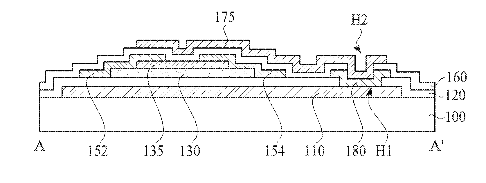
[0044]FIG. 2A is a plane view illustrating a thin film transistor substrate according to the first embodiment of the present invention. FIG. 2B is a cross sectional view along A-A′ of FIG. 2A.

[0045]First, the thin film transistor substrate according to the first embodiment of the present invention will be described with reference to FIG. 2A.

[0046]As shown in FIG. 2A, a thin film transistor (T) and a contact portion 180 are formed on the thin film transistor substrate 100, wherein the thin film transistor (T) functions as a switching element for controlling an operation of each pixel, or a driving element for driving each pixel.

[0047]The thin film transistor (T) includes a lower gate electrode 110, an etch stopper layer 135, a source electrode 152, a drain ...

second embodiment

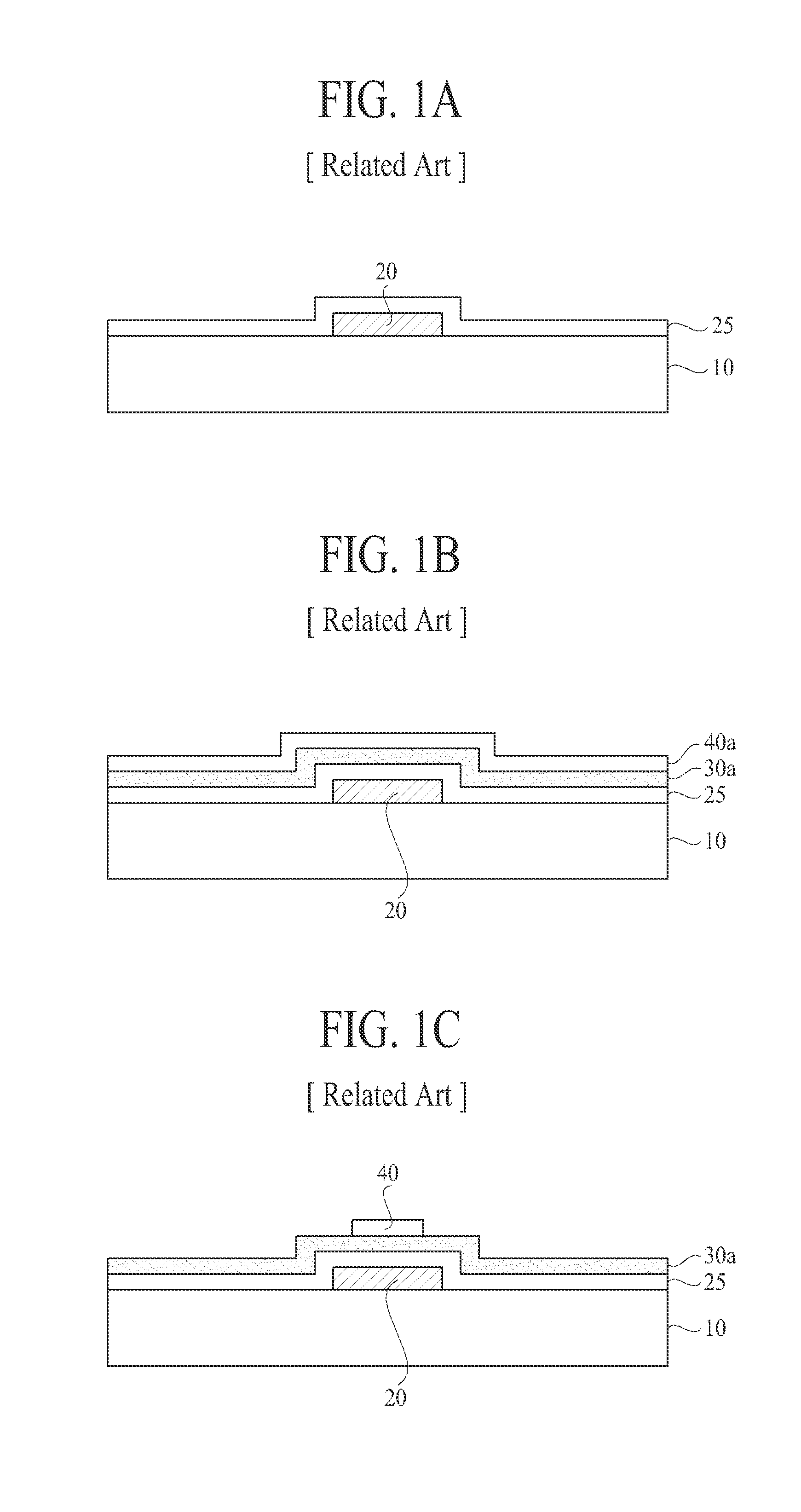
[0082]In the above description for the first embodiment of the present invention, the etch stopper layer 135 is formed only in the channel region on the active layer 130, whereby the source electrode 152 and drain electrode 154 cover all regions of the active layer 130 except the channel region.

[0083]However, in case of the second embodiment of the present invention, an etch stopper layer 135 is formed not only in the channel region but also in regions except the channel region on an active layer 130, whereby the etch stopper layer 135 covers the active layer 130.

[0084]Hereinafter, the thin film transistor substrate according to the second embodiment of the present invention will be described in more detail with reference to FIGS. 5 and 6. For the following description, wherever possible, the same reference numbers will be used throughout the drawings to refer to the same or like parts as those of the first embodiment of the present invention.

Thin Film Transistor Substrate

[0085]FIG....

first modified embodiment

[0123]In the above first and second embodiments of the present invention, the contact portion 180 for electrically connecting the lower gate electrode 110 and upper gate electrode 175 of the thin film transistor (T1) is formed in the island shape. However, according to the first modified embodiment of the present invention, as shown in FIGS. 7A and 7B, a contact portion 180 may be formed as a single body with a source electrode or drain electrode (S or D) of a thin film transistor (T2).

[0124]Also, in the above first and second embodiments of the present invention, the source electrode 152 is connected with the data line 150. However, according to the first modified embodiment of the present invention, a source electrode 152 may be connected with a power line.


PUM


Abstract

Disclosed is a thin film transistor substrate which facilitates to improve output and transfer characteristics of thin film transistor, wherein the thin film transistor substrate comprises a thin film transistor comprising a lower gate electrode on a substrate, an active layer on the lower gate electrode, source and drain electrodes on the active layer, and an upper gate electrode on the source electrode, drain electrode and active layer, the upper gate electrode for covering a channel region defined by the source and drain electrodes; and a contact portion for electrically connecting the lower gate electrode with the upper gate electrode.

Description

CROSS REFERENCE TO RELATED APPLICATIONS[0001]This application claims the benefit of the Korean Patent Application No. 10-2012-0088565 filed on Aug. 13, 2012, which is hereby incorporated by reference as if fully set forth herein.BACKGROUND[0002]1. Field of the Invention[0003]The present invention relates to a display device, and more particularly, to a thin film transistor applied to a display device.[0004]Discussion of the Related Art[0005]A thin film transistor (TFT) is used as a switching element for controlling an operation of each pixel or a driving element for driving each pixel in a display device such as a liquid crystal display (LCD) or an organic light emitting device (OLED).[0006]The thin film transistor includes a gate electrode, an active layer, and source / drain electrodes. Based on an arrangement of the electrodes, the thin film transistor may be classified into a staggered structure and a coplanar structure.[0007]In case of the staggered structure, the gate electrode ...

Claims


Application Information

Patent Timeline
Patent Type & Authority Applications(United States)
IPC IPC(8): H01L29/786H01L51/50H01L29/66
CPCH01L29/786H01L51/50H01L29/66742H01L29/78633H01L29/78648H01L29/7869H01L29/41733H01L29/66969H10K50/00H10K59/1213H10K59/131
Inventor SHIM, JONG SIKNAM, WOO JINSHIN, HONG JAECHANG, MIN KYU
Owner LG DISPLAY CO LTD
Why Eureka
Try Eureka