Bipolar transistor

Active Publication Date: 2014-02-13
X FAB SEMICON FOUNDRIES
View PDF13 Cites 2 Cited by
  • Summary
  • Abstract
  • Description
  • Claims
  • Application Information

AI Technical Summary

Benefits of technology

[0007]Some embodiments of the present invention aim to address the problem of recombination current and consequently improve gain linearity in a bipolar junction transis

Problems solved by technology

A problem with bipolar junction transistors is that the high base recomb

Method used


Image

  • Bipolar transistor
  • Bipolar transistor
  • Bipolar transistor

Examples


Example

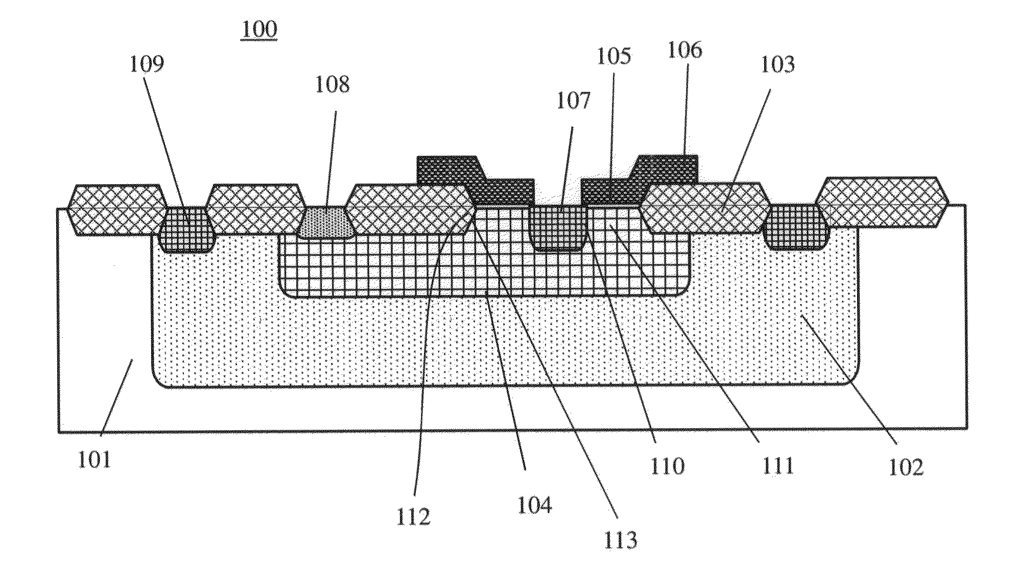
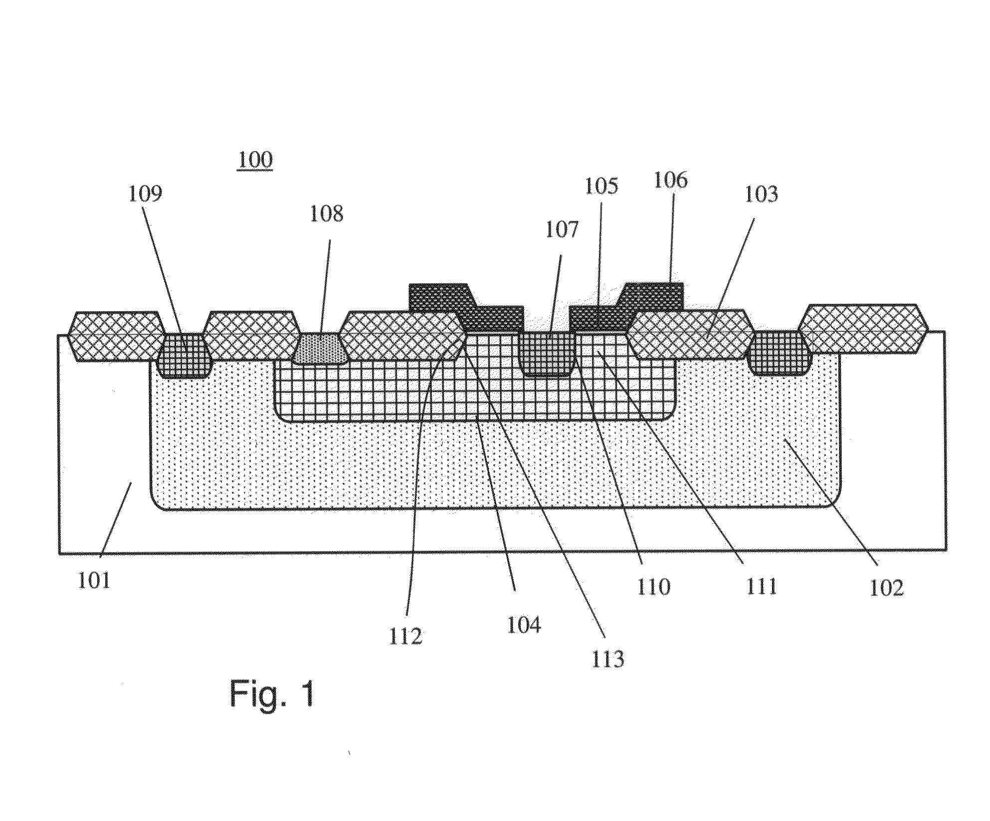
[0038]FIG. 1 shows a cross-sectional view of a bipolar junction transistor 100 according to an embodiment of the present invention. The bipolar junction transistor 100 shown in FIG. 1 is an NPN transistor formed in a p-type substrate 101. The transistor 100 comprises a deep N well region 102 formed within the p-type substrate 101. A P well region 104 is formed within the deep N well region 102, and an N+ region 107 is formed within the P well 104. These wells form the collector 102, base 104, and emitter 107 respectively of the bipolar junction transistor. A base contact 108 is formed in the base region and a collector contact 109 is formed in the collector region. On the surface of the substrate in between the contacts, LOCOS / STI field oxide separators 103 are formed. These separate the base contact 108 and the collector contact 109 on the surface of the transistor 100. The field oxide also runs from the base contact 108 towards the emitter 107 leaving a portion of the surface of t...


PUM


Abstract

A bipolar junction transistor is provided with an emitter region, an oxide region, a base region and a collector region. The base region is located between the emitter region and the oxide region and has a junction with the emitter region and an interface with the oxide region. An at least partially conductive element such as metal or silicon is positioned to overlap with at least part of the junction between the base region and the emitter region, thereby forming a gate. The gate also overlaps with at least part of the interface between the base region and the oxide region. When a suitable bias voltage is applied to the gate, the gain of the transistor can be increased.

Description

CROSS REFERENCE TO RELATED APPLICATION[0001]This application is a continuation-in-part of International Patent Application Number PCT / EP2011 / 055731 filed on 12 Apr. 2011, the entire contents of which are herein incorporated by reference.TECHNICAL FIELD[0002]The present invention relates to semiconductor devices. More specifically, the present invention relates to a bipolar transistor. Embodiments of the invention exhibit an improved linearity of the gain, or substantially linear gain, with respect to bias current by reduction of the base-emitter recombination current. Some embodiments exhibit an increased gain of the transistor.BACKGROUND[0003]Bipolar junction transistors are constructed from doped semiconductor material and are often used in switching and amplifying applications.[0004]A problem with bipolar junction transistors is that the high base recombination current is a main contributor to degradation of low current gain. Under typical operation of e.g. an NPN transistor, ele...

Claims


Application Information

Patent Timeline
IPC IPC(8): H01L29/73
CPCH01L29/73H01L29/402H01L29/66272H01L29/66295H01L29/7322
Inventor TONER, BRENDANCAO, XUEZHOUFANG, FREDTAN, CHUAN CHIEN
Owner X FAB SEMICON FOUNDRIES
Why Eureka
Try Eureka