Semiconductor device and power control method therefor

a technology of semiconductor devices and power control methods, which is applied in the direction of pulse automatic control, pulse technique, power consumption reduction, etc., can solve the problems of increasing circuit power consumption, occupying almost the entire chip after several years, and increasing circuit scale, so as to achieve the effect of reducing the charge power of a semiconductor devi

Inactive Publication Date: 2014-02-13
CANON KK
View PDF2 Cites 3 Cited by
  • Summary
  • Abstract
  • Description
  • Claims
  • Application Information

AI Technical Summary

Benefits of technology

[0016]According to the aspect, it is possible to implement charge recycle for effectively reducing the charge power of a semiconductor device.

Problems solved by technology

With an increase in circuit scale, the power consumed by the circuit also tends to increase.
On the other hand, the static power means power generated by a leak current which flows through the transistor even without a signal change.
Also, a circuit block which requires power shutdown in a chip is expected to increase steadily and therefore occupy almost the entire chip after several years.
In other words, it is necessary to supply a charge corresponding to the capacitance of the circuit block, thus consuming power upon charging.
In a chip with its entire configuration built by a circuit block to undergo power shutdown, an increase in charge power is more non-negligible than a reduction in static power, and this may inhibit the power reduction effect by the power shutdown technique.
However, such timing control operations cannot cope with the case wherein, for example, the timing shifts due, for example, to individual variations of transistors in a chip, which occur upon evolution of technology nodes.
Also, power that can be reduced originally may waste as charges cannot be optimally distributed to a capacitance.

Method used


Image

  • Semiconductor device and power control method therefor
  • Semiconductor device and power control method therefor
  • Semiconductor device and power control method therefor

Examples


embodiment

Modification of Embodiment

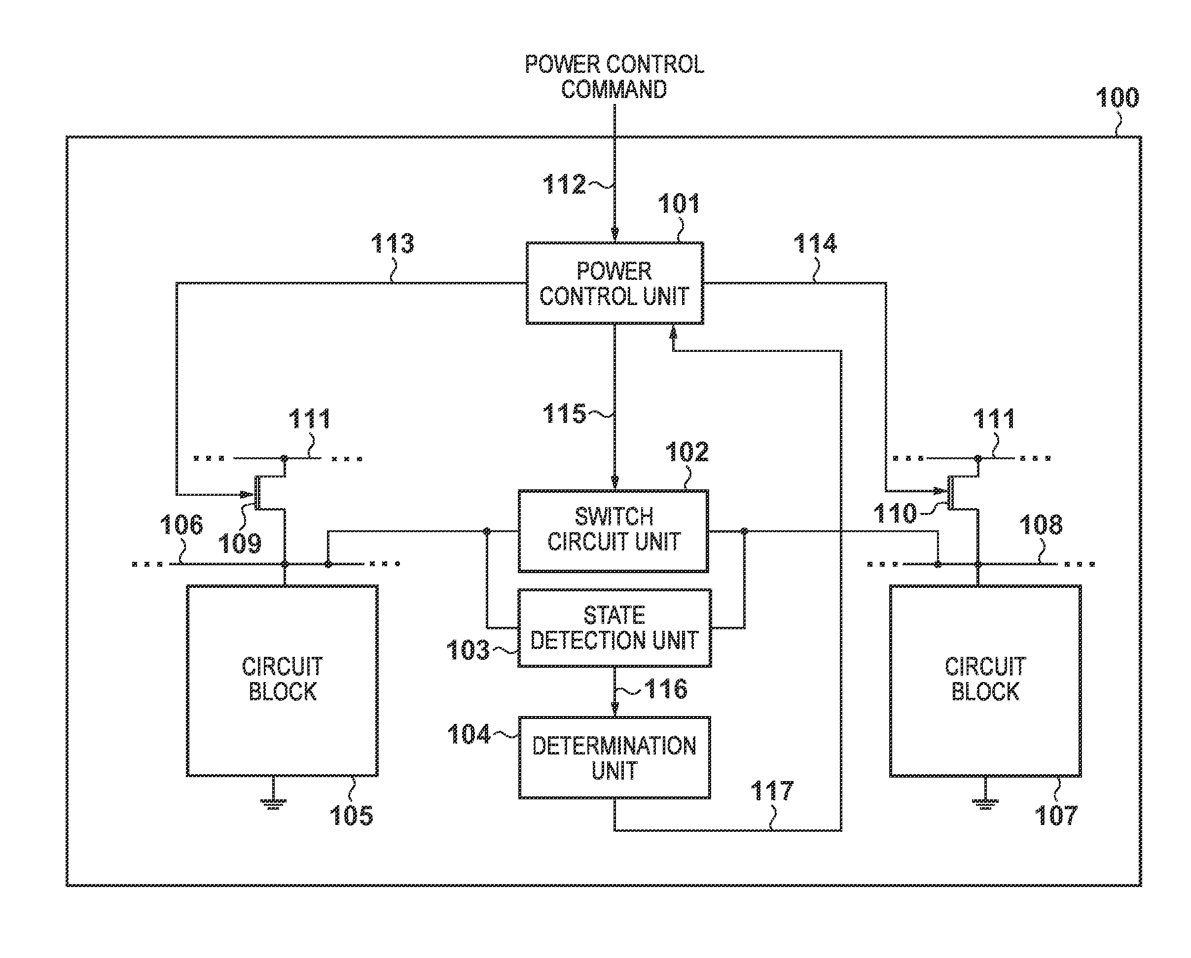
[0071]An example in which the present invention is applied to a semiconductor device 100 including two circuit blocks 105 and 107 has been described above. However, the present invention is applicable to a semiconductor device including a plurality of circuit blocks. In this case, a first switch is disposed for each circuit block. Also, a second switch is disposed between two adjacent circuit blocks.

[0072]The present invention is also applicable to a semiconductor device including four circuit blocks, and four second switches disposed to connect these circuit blocks in a ring shape. If the power control unit 101 receives a command which sets the first circuit block in a power supply state, and the second to fourth circuit blocks in a power supply state, it performs the following control operation. The first switch connected to the local wiring of the first circuit block is set in an open state, and all the second switches are set in a closed state. Then, wh...


PUM


Abstract

A semiconductor device comprises a plurality of circuit blocks, a plurality of local wirings which supply power to the plurality of circuit blocks, respectively, a global wiring which supplies the power to the plurality of local wirings, a plurality of first switches which are disposed between the plurality of local wirings, respectively, and the global wiring, and a second switch which is disposed between two local wirings. A power control unit controls open / close of the plurality of first switches and the second switch based on the potential difference between the two local wirings.

Description

BACKGROUND OF THE INVENTION[0001]1. Field of the Invention[0002]The present invention relates to power control for a semiconductor device.[0003]2. Description of the Related Art[0004]As the process becomes finer with advances in semiconductor manufacturing technology, miniaturization of transistor elements has made rapid progress. As a result, the number (the degree of integration) of transistors that can be mounted on a chip with the same area increases, so the circuit scale has expanded to 10 or more times in several recent years. With an increase in circuit scale, the power consumed by the circuit also tends to increase. The power consumed by the circuit includes dynamic power and static power.[0005]The dynamic power means power generated by a current which flows through the transistor due to a signal change. The dynamic power can be reduced by suppressing a signal change, and the clock gating technique of shutting down clock supply to the circuit for a period in which a circuit ...

Claims


Application Information

Patent Timeline
Patent Type & Authority Applications(United States)
IPC IPC(8): H03K3/012
CPCH03K3/012H03K19/0013H03K19/0016
Inventor MINAKAWA, TAKUYA
Owner CANON KK
Why Eureka
Try Eureka