Mos resistor apparatus and methods

a resistor and mos technology, applied in the field of mos resistor apparatus and methods, can solve the problems of inconvenient implementation, inconvenient use, and inability to accurately measure the accuracy of the resistor, etc., and achieve the effect of not constant resistance associated with the resistor formed using mos transistor operating in the linear region

Active Publication Date: 2014-02-20
TEXAS INSTR INC
View PDF1 Cites 13 Cited by
  • Summary
  • Abstract
  • Description
  • Claims
  • Application Information

AI Technical Summary

Problems solved by technology

However, the accuracy of this approach is limited to the accuracy of the resistor, per Ohm's Law.
However, large polysilicon resistors occupy a large wafer area and may thus be expensive to implement.
Unfortunately it can be seen that, for a given process and geometry, the resistance associated with a resistor formed using a MOS transistor operating in the linear region is not constant.

Method used


Image

  • Mos resistor apparatus and methods
  • Mos resistor apparatus and methods
  • Mos resistor apparatus and methods

Examples


Embodiment Construction

[0018]FIG. 1 is a prior-art circuit diagram of a MOS resistor. A current I(REF) 102 is injected from a current source 105 into the current channel of a diode-connected MOS transistor 110. I(REF) is selected to create a bias voltage V(DI) 115 to bias the MOS transistor 120 to operate in the linear region. A MOS resistor is thus created between the source and drain terminals 125 and 130, respectively. Turning again to the equation for the MOS resistor:

R(DS)=1kWL(V(GS)-V(TH)-V(DS) / 2

It can be seen that the resistance value retains a dependency upon the voltage V(DS) applied across the resistor terminals even as the gate voltage is held constant at V(DI).

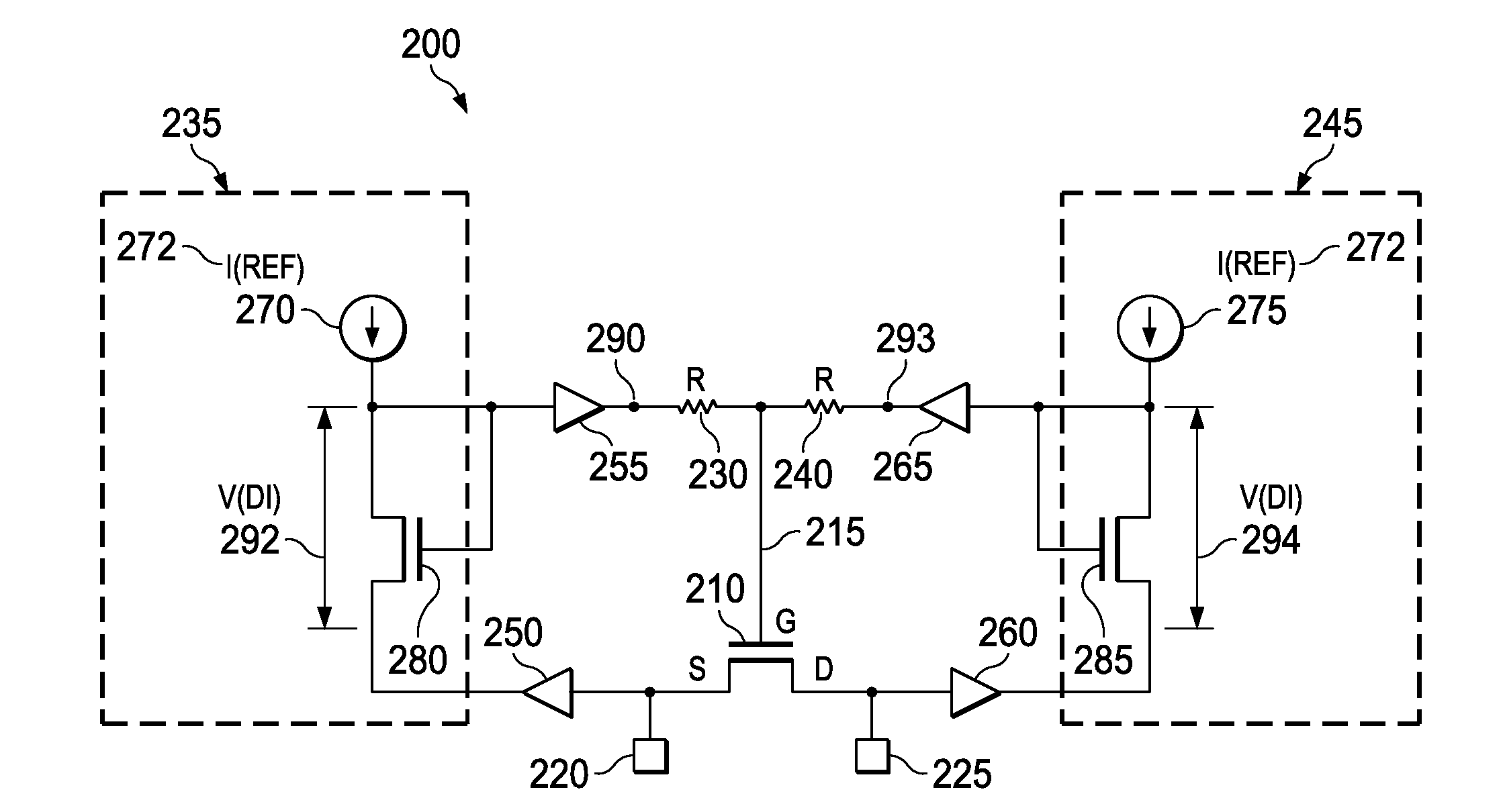
[0019]FIG. 2 is a circuit diagram of a MOS resistor 200 according to various example aspects of the invention. The MOS resistor 200 includes a MOS transistor 210 with a gate terminal 215. The MOS resistor 200 also includes two resistor terminals 220 and 225. One MOS resistor terminal is associated with the MOS transistor source and one M...


PUM


Abstract

Apparatus and methods disclosed herein implement a MOS resistor using the current channel of a MOS transistor. The MOS resistance R(DS) is dependent upon MOS transistor geometry and nominal gate voltage. MOS resistor terminal-to-gate voltages are averaged and applied to the MOS transistor gate such as to maintain the MOS resistor terminal voltage to current ratio, resulting in a substantially constant R(DS). R(DS) is also compensated for temperature and process variations by adjusting gate voltages via negative feedback methods.

Description

PRIORITY CLAIM[0001]This application claims the benefit of priority under 35 U.S.C. §119(e) to U.S. Provisional Patent Application Ser. No. 61 / 682,840 titled “Large, Linear, PT-insensitive, Low-leakage MOS Resistor” filed on Aug. 14, 2012 and incorporated herein by reference in its entirety.TECHNICAL FIELD[0002]Structures and methods described herein relate to semiconductor integrated resistors, including resistors implemented with metal oxide semiconductor (MOS) transistors.BACKGROUND INFORMATION[0003]Some integrated electronic circuits may utilize electronic resistors for proper operation. For example, a circuit for measuring an electrical current may be simplified by measuring the voltage drop across a resistor through which the test current is flowing. The latter approach may prove more economical than methods of measuring the current directly. However, the accuracy of this approach is limited to the accuracy of the resistor, per Ohm's Law.[0004]In one approach, a length of dope...

Claims


Application Information

Patent Timeline
Patent Type & Authority Applications(United States)
IPC IPC(8): H03H11/02
CPCH03H11/02H03H11/245G11C5/147
Inventor POLLEY, ARUP
Owner TEXAS INSTR INC
Why Eureka
Try Eureka