Substrate processing device and substrate processing method for carrying out chemical treatment for substrate

a substrate processing and processing device technology, applied in semiconductor/solid-state device manufacturing, basic electric elements, electric devices, etc., can solve the problems of reducing the yield or trouble of the substrate processing device itself, reducing the etching rate, and reducing the uniformity of the etching width. , to achieve the effect of suppressing deterioration, reducing the chemical treatment width and reducing the chemical treatment efficiency

Inactive Publication Date: 2014-02-20
DAINIPPON SCREEN MTG CO LTD
View PDF14 Cites 20 Cited by
  • Summary
  • Abstract
  • Description
  • Claims
  • Application Information

AI Technical Summary

Benefits of technology

[0019]Therefore, it is an object of the present invention to provide a technique capable of reducing a chemical treating width while suppressing deterioration in each of uniformity of a chemical treating width (an etching width or the like) and chemical treating efficiency (an etching rate or the like).

Problems solved by technology

In cases where the film is formed on the back surface of the substrate or the peripheral edge part of the upper surface of the substrate, a thin film formed on the peripheral edge part of the upper surface of the substrate may be peeled by contact with another device at a subsequent step to the film forming step, and may cause reduction in yield or a trouble of a substrate processing device itself.
According to the method, although an average etching width can be reduced, uniformity of the etching width is deteriorated, for example, the amount of wraparound of the processing liquid to the peripheral edge part is controlled with difficulty so that a portion to be etched locally and greatly appears.
Furthermore, there is also a problem in that the temperatures of the peripheral edge part and the processing liquid in the peripheral edge part are lowered, resulting in reduction in an etching rate.
However, there is a problem in that the etching rate in the peripheral edge part of the substrate is reduced due to decrease in the amount of the processing liquid and reduction in the temperature of the processing liquid in a pipe due to the decrease.
These are problems which are not limited to the etching using the etchant, but are caused in general processing for carrying out a chemical treatment for a substrate by using a processing liquid having a reaction rate increased with a rise in a temperature.

Method used


Image

  • Substrate processing device and substrate processing method for carrying out chemical treatment for substrate
  • Substrate processing device and substrate processing method for carrying out chemical treatment for substrate
  • Substrate processing device and substrate processing method for carrying out chemical treatment for substrate

Examples


embodiment

Preferred Embodiment

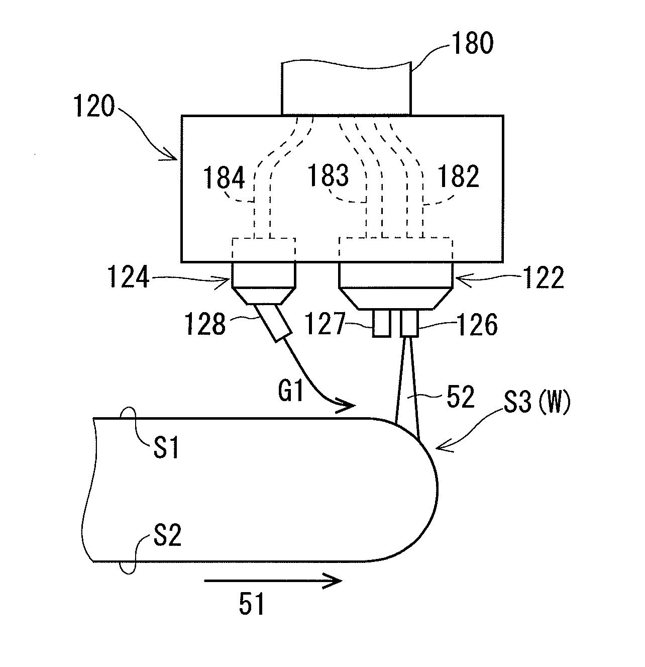
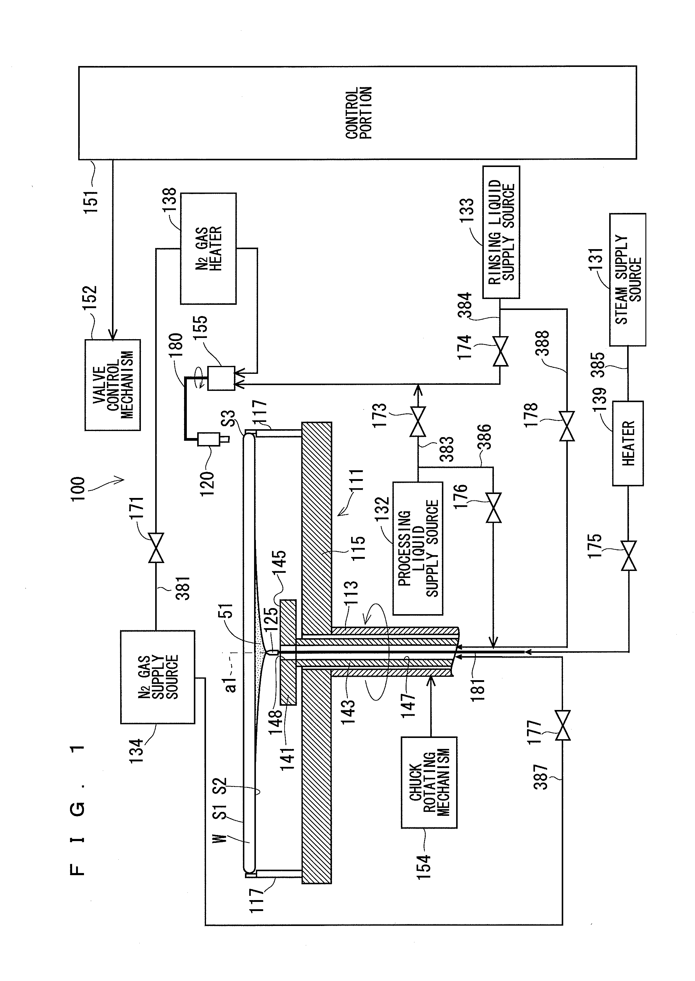
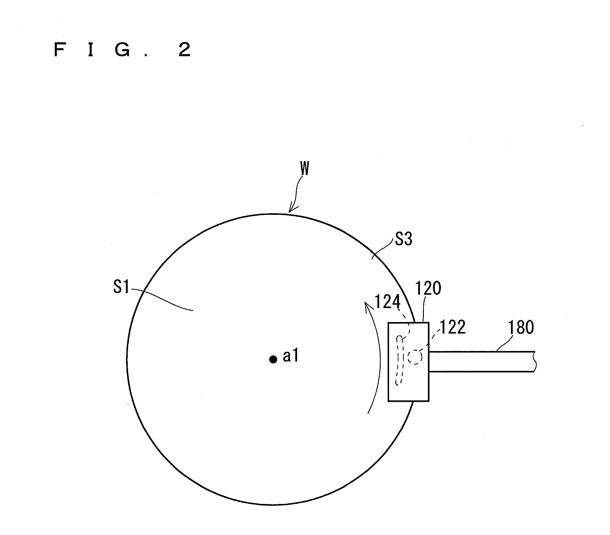
[0031]FIG. 1 is a view schematically showing an example of a schematic structure of a substrate processing device 100 according to a preferred embodiment. The substrate processing device 100 carries out a chemical treatment for a substrate by using a processing liquid having a reaction rate increased with a rise in temperature. More specifically, the substrate processing device 100 performs etching for a peripheral edge part (also referred to as an “upper surface peripheral edge part”) S3 of a substrate W such as a semiconductor wafer in a front surface (also referred to as an “upper surface”) S1 of the substrate W by using an etchant as a processing liquid for a chemical treatment, thereby removing a thin film (an unnecessary object) formed on the upper surface peripheral edge part S3. The upper surface peripheral edge part S3 is a ring-shaped region having a width of 0.5 to 3.0 mm from a peripheral edge of the substrate W in the upper surface S1 of the substrat...


PUM

PropertyMeasurementUnit
diameteraaaaaaaaaa
widthaaaaaaaaaa
widthaaaaaaaaaa

Abstract

It is an object to reduce a chemical treating width in a peripheral edge part of a substrate while suppressing deterioration in each of uniformity of the chemical treating width and processing efficiency. In order to achieve the object, a substrate processing device for carrying out a chemical treatment for a substrate using a processing liquid having a reaction rate increased with a rise in temperature includes a substrate holding portion, a rotating portion for rotating the substrate held in the substrate holding portion in a substantially horizontal plane, a heating portion for injecting heating steam to a central part of a lower surface of the substrate to entirely heat the substrate, and a peripheral edge processing portion for supplying the processing liquid from above to a peripheral edge part of the substrate heated by the heating portion, thereby carrying out a chemical treatment for the peripheral edge part.

Description

BACKGROUND OF THE INVENTION[0001]1. Field of the Invention[0002]The present invention relates to a substrate processing device and a substrate processing method for supplying a processing liquid to a substrate to carry out a chemical treatment such as etching while rotating the substrate. The substrate to be processed includes substrates, for example, a semiconductor wafer, a substrate for an optical disk, a substrate for a magnetic disk, a substrate for a magneto-optical disk, a substrate for a photomask, a substrate for a solar cell, and the like.[0003]2. Description of the Background Art[0004]Although a series of processing steps for a substrate such as a semiconductor wafer have a plurality of film forming steps for forming a thin film of a metal, a photoresist or the like on a front surface (“an upper surface”) of the substrate, a film is also formed on a back surface (“a lower surface”) of the substrate or a peripheral edge part of the upper surface of the substrate at the fil...

Claims


Application Information

Patent Timeline
Patent Type & Authority Applications(United States)
IPC IPC(8): H01L21/306H01L21/67
CPCH01L21/6708H01L21/30604H01L21/02087H01L21/0209H01L21/32134H01L21/67028H01L21/302H01L21/306H01L21/02035H01L21/67109H01L21/68792
Inventor SHIBAYAMA, NOBUYUKI
Owner DAINIPPON SCREEN MTG CO LTD
Why Eureka
Try Eureka