

Compound semiconductor integrated circuit
- Summary
- Abstract
- Description
- Claims
- Application Information
AI Technical Summary
Benefits of technology
Problems solved by technology
Method used
Image

Examples
Embodiment Construction
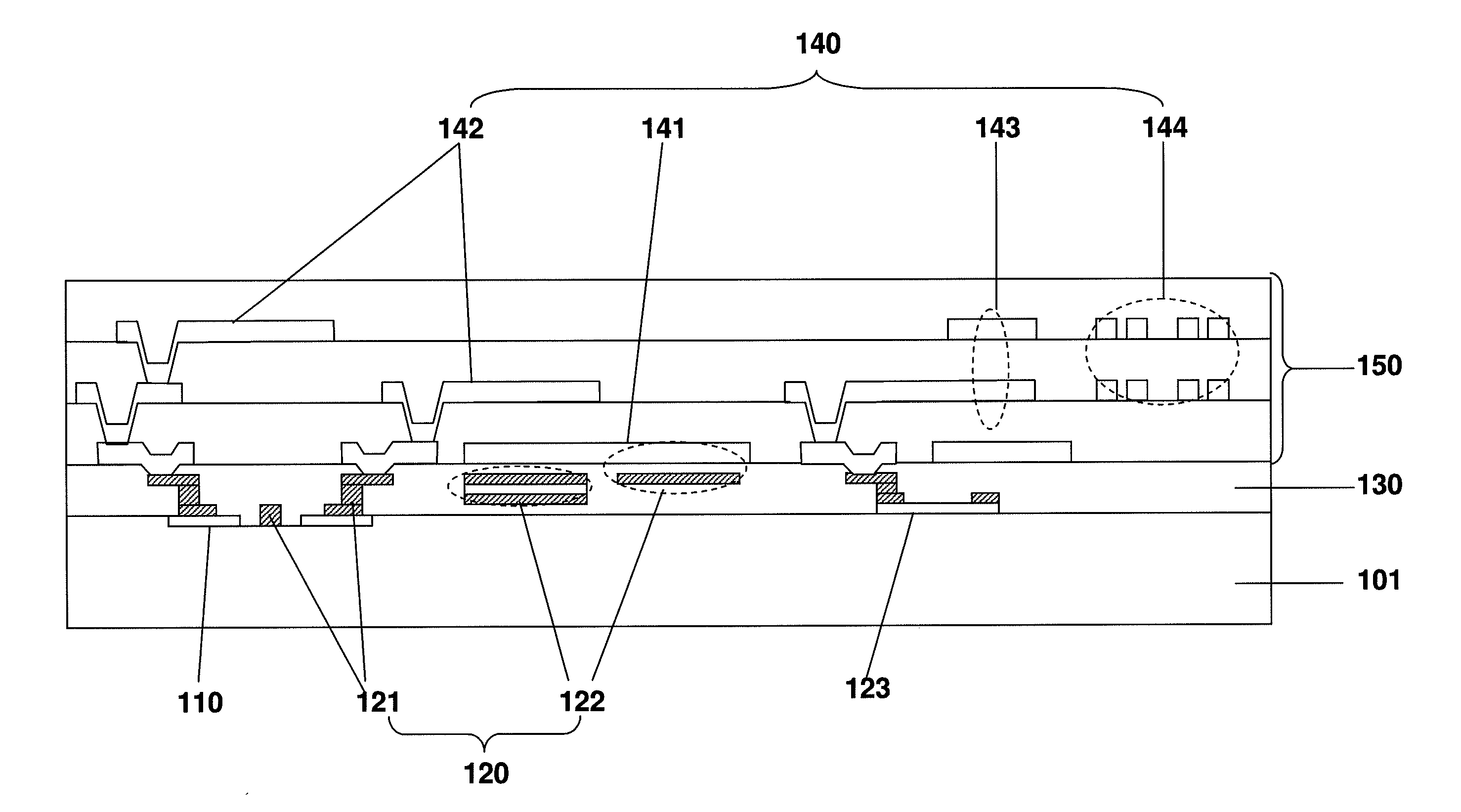
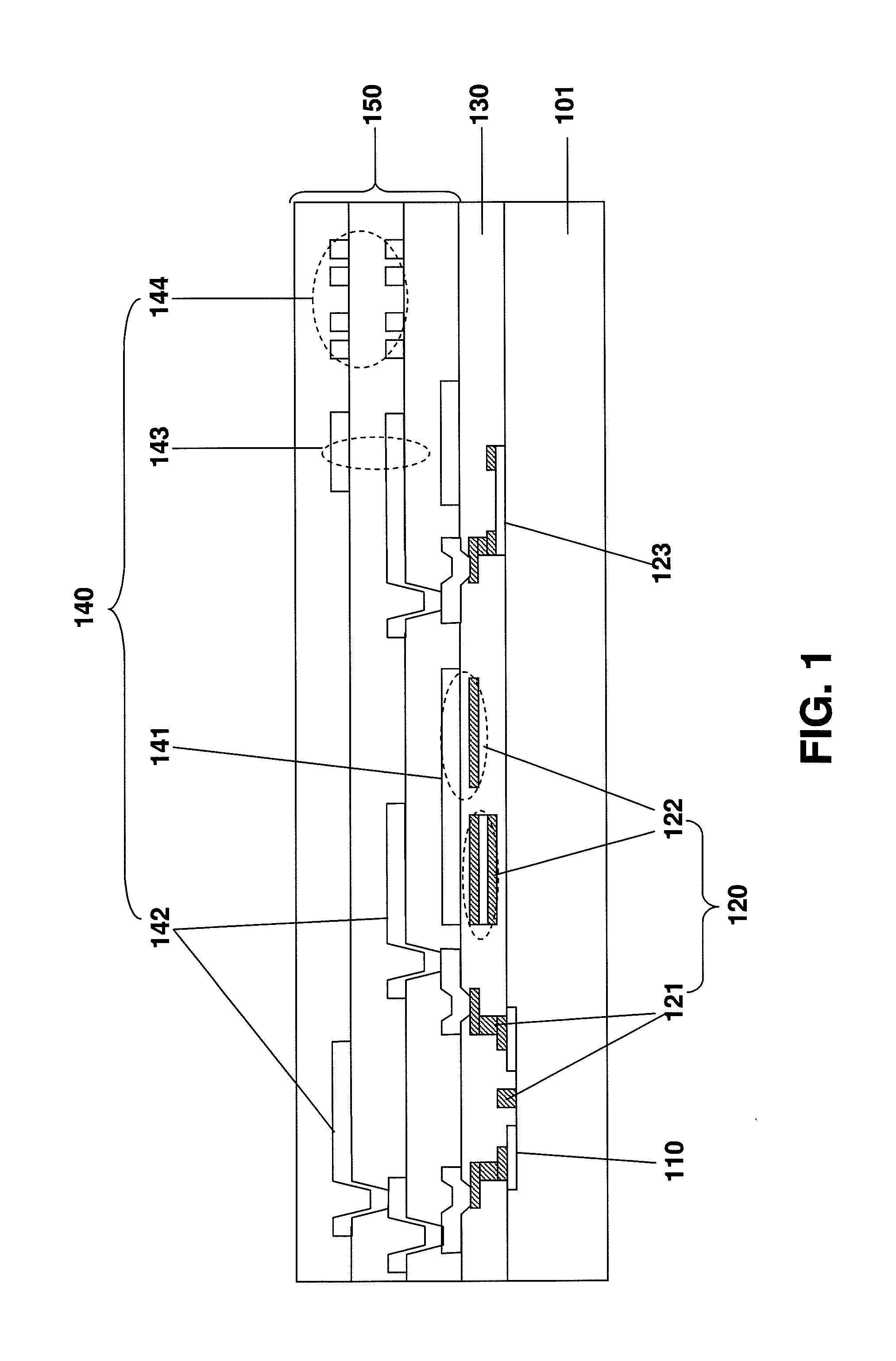
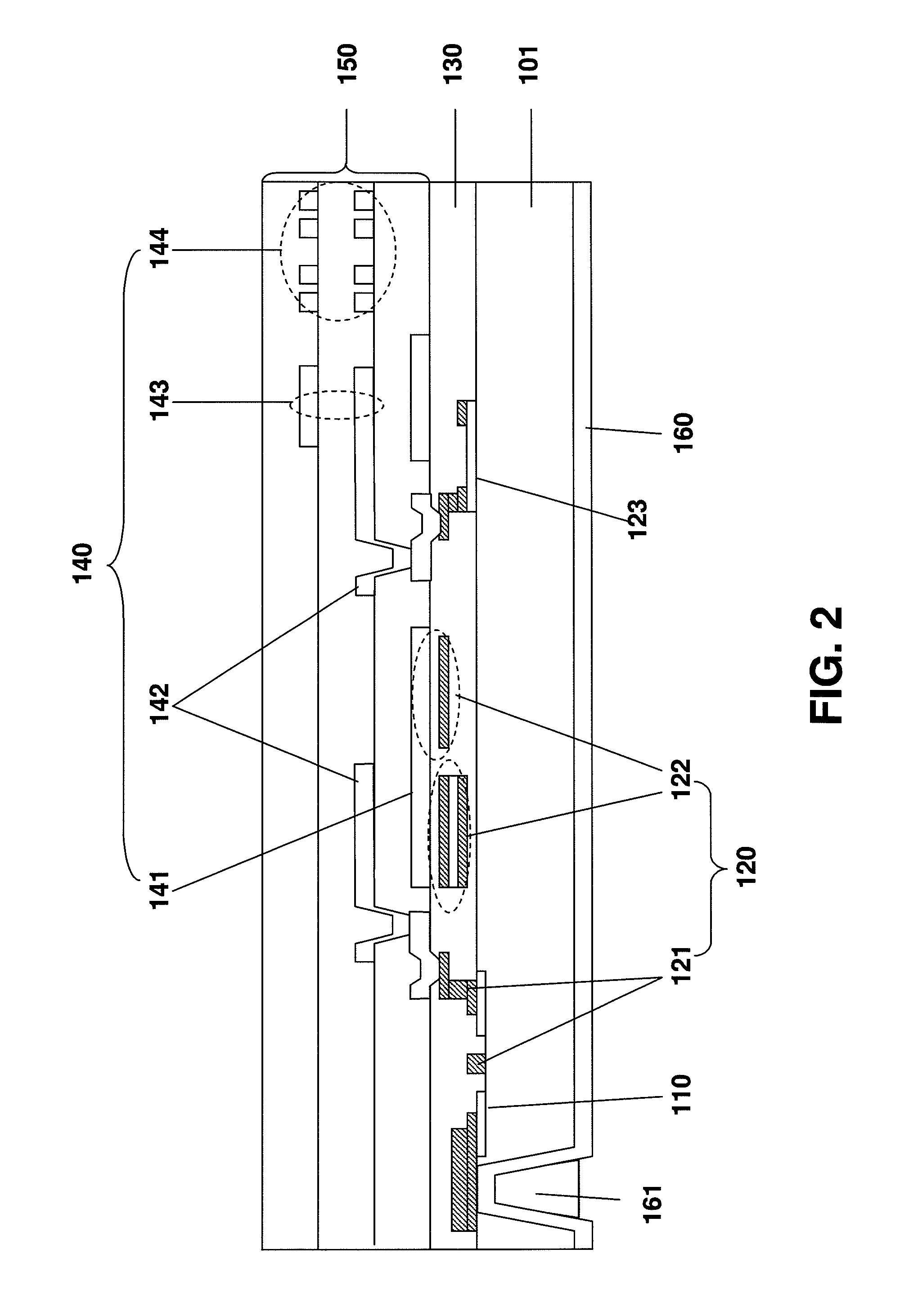
[0022]FIG. 1 is a schematic showing the cross-sectional view of an embodiment of a compound semiconductor integrated circuit according to the present invention, which comprises a substrate 101, at least one compound semiconductor electronic device 110, a first metal layer 120, a protection layer 130, a plurality of second metal layers 140, and at least one dielectric layer 150. The substrate 101 is made of semi-insulating or insulating material such as GaAs, SiC, or sapphire. The compound semiconductor electronic device 110 is formed on the substrate 101. The compound semiconductor electronic device 110 can be an FET or an HBT made mainly of GaAs. The compound semiconductor electronic device 110 can also be a GaN FET. The first metal layer 120 is formed on the compound semiconductor electronic device 110 and is at least partly electrically connected to the compound semiconductor electronic device 110. The first metal layer 120 can be used to form passive electronic components such a...
PUM
 Abstract
Description
Claims
Application Information