Wiring board and manufacturing method of wiring board

Active Publication Date: 2014-02-27
SONY CORP
View PDF2 Cites 4 Cited by
  • Summary
  • Abstract
  • Description
  • Claims
  • Application Information

AI Technical Summary

Benefits of technology

The patent text is discussing a concern that there may be a risk of cracking or breaking in the edge of a wiring board when it is exposed on surfaces in both coreless and core type wiring boards. This may lead to chipping, which can cause damage to the electronic components. The technical effect of the patent is to address this concern and provide a solution to prevent cracking or breaking in the wiring board edge.

Problems solved by technology

However, since the laminate is exposed on surfaces in both coreless type and core type wiring boards, cracking or breaking easily occurs particularly in an edge of a board when external force derived from impact, shaking, or the like is exerted thereon, and thus there is concern that chipping may occur.
There is a possibility of a wiring layer being exposed according to the degree of such chipping, and accordingly, a worsening manufacturing yield and low reliability are concerns.
In addition, since such a coreless type wiring board has low rigidity overall as described above, warping easily occurs, and accordingly, a defect in flip-chip connection may be caused.
If this stress is strong, a crack occurs in a bonding portion of the IC chip, there is a possibility of an open defect or the like, and thereby a high manufacturing yield and reliability are difficult to realize.

Method used


Image

  • Wiring board and manufacturing method of wiring board
  • Wiring board and manufacturing method of wiring board
  • Wiring board and manufacturing method of wiring board

Examples


Embodiment Construction

)

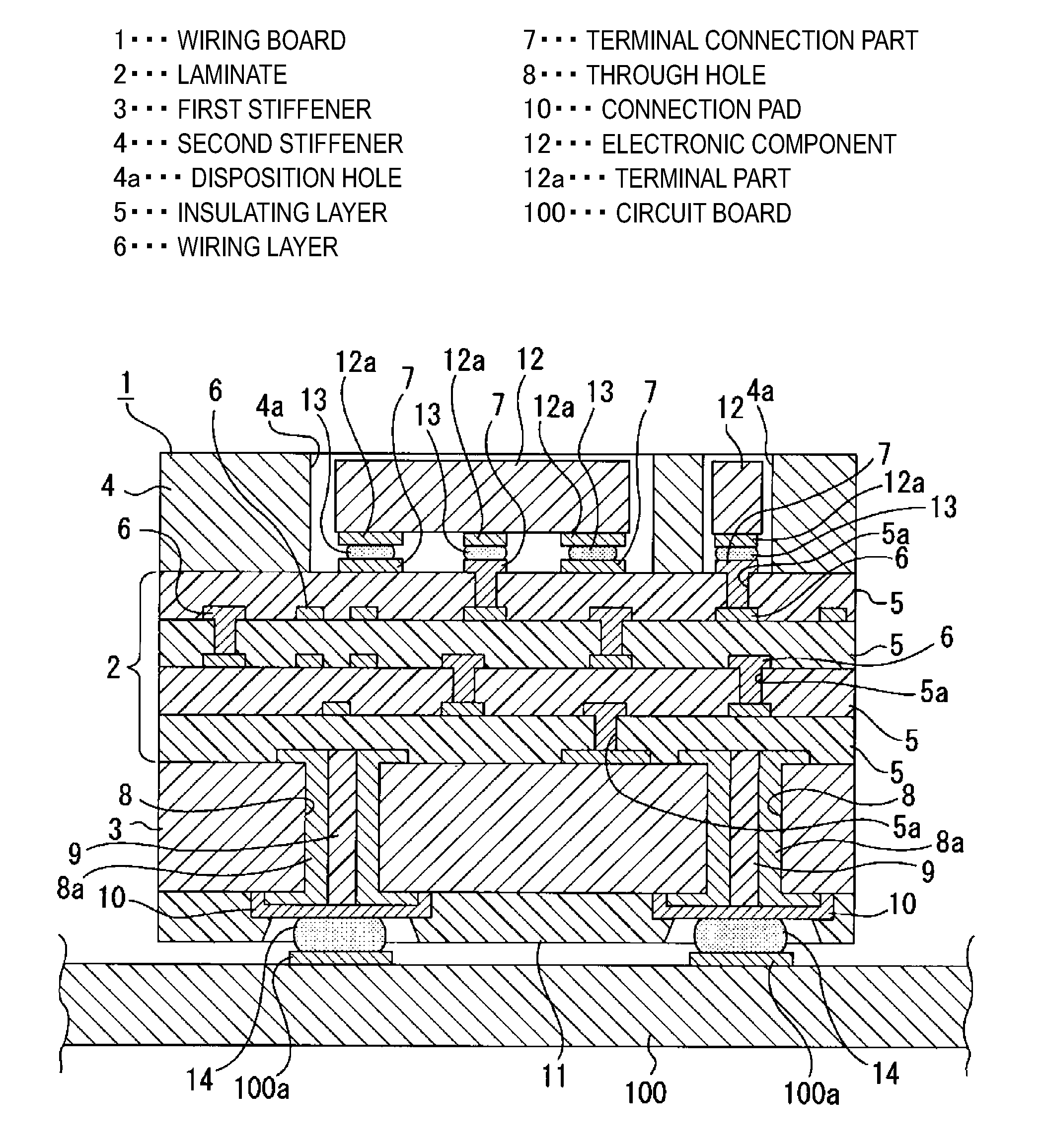
[0044]Hereinafter, preferred embodiments of the present technology will be described in detail with reference to the appended drawings. Note that, in this specification and the appended drawings, structural elements that have substantially the same function and structure are denoted with the same reference numerals, and repeated explanation of these structural elements is omitted.

[0045]Hereinafter, preferred embodiments for implementing a wiring board and a manufacturing method of a wiring board of an embodiment of the present technology will be described with reference to the appended drawings.

[0046]A wiring board is a wiring board that is a so-called semiconductor package having a structure with a plurality of laminated layers.

[0047]In description below, in a wiring board, front to back, top to bottom, and left to right directions are indicated based on a laminating direction of each part which is set to be the top to bottom direction.

[0048]It should be noted that the front to ba...


PUM


Abstract

There is provided a wiring board including a first stiffener, one face of which is bonded to a circuit board, a second stiffener having a disposition hole in which an electronic component is disposed, and a laminate that is formed by laminating a plurality of insulating layers and a plurality of wiring layers between the other face of the first stiffener and one face of the second stiffener, and includes a terminal connection part that is connected to the wiring layers, positioned in the disposition hole, and connected to a terminal part of the electronic component.

Description

BACKGROUND[0001]The present technology relates to the technical field of a wiring board and a manufacturing method of a wiring board. Specifically, the present technology relates to the technical field for improving flip-chip connectability and preventing occurrence of chipping in an IC (Integrated Circuit) chip by forming a laminate that is obtained by laminating a plurality of insulating layers and a plurality of wiring layers between a first stiffener and a second stiffener and thereby suppressing occurrence of warping.[0002]Along with the recent speed-up and high performance of electronic components (IC chips) used as microprocessors, or the like of a computer, the number of terminals tends to increase and pitches between terminals tend to be narrow. Generally, a large number of terminal parts are provided on the bottom of an IC chip in an array form.[0003]Such terminal parts of an IC chip have a large difference in pitch with respect to connection terminals formed on a circuit ...

Claims


Application Information

Patent Timeline
IPC IPC(8): H05K1/18H05K3/46
CPCH05K3/4644H05K1/184H05K1/183H05K3/4602H05K3/4697H05K1/0271H05K2201/09136H05K2201/1009H01L2224/16225H01L2924/15311
Inventor SATO, JUNICHI
Owner SONY CORP
Why Eureka
Try Eureka