Semiconductor device and method of fabricating the same

a technology of semiconductor devices and semiconductors, applied in the direction of semiconductor devices, basic electric elements, electrical equipment, etc., can solve the problem of increasing the capacity of drams, and achieve the effect of reducing the resistance of gates

Active Publication Date: 2014-03-06
SK HYNIX INC
View PDF9 Cites 29 Cited by
  • Summary
  • Abstract
  • Description
  • Claims
  • Application Information

AI Technical Summary

Benefits of technology

[0022]spacer-etching on the According to the exemplary embodiment of the inventive concept, GIDL is improved and gat...

Problems solved by technology

In recent years, although demands on large capacity of dynamic random access memories (DRAMs) hav...

Method used


Image

  • Semiconductor device and method of fabricating the same
  • Semiconductor device and method of fabricating the same
  • Semiconductor device and method of fabricating the same

Examples


Embodiment Construction

”.

BRIEF DESCRIPTION OF THE DRAWINGS

[0024]The above and other aspects, features and other advantages of the subject matter of the present disclosure will be more clearly understood from the following detailed description taken in conjunction with the accompanying drawings, in which:

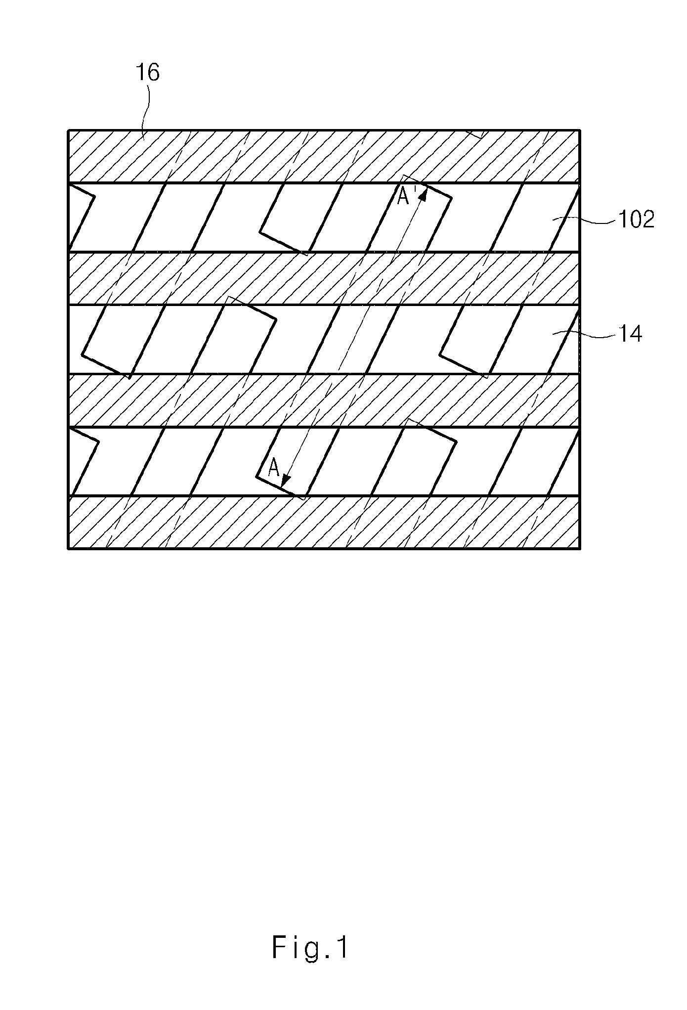
[0025]FIG. 1 is a plan view illustrating a 6 F2 structure to which a semiconductor device according to exemplary embodiments of the inventive concept is applied;

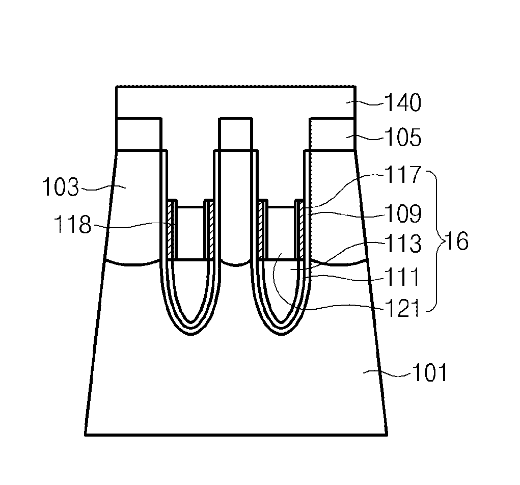
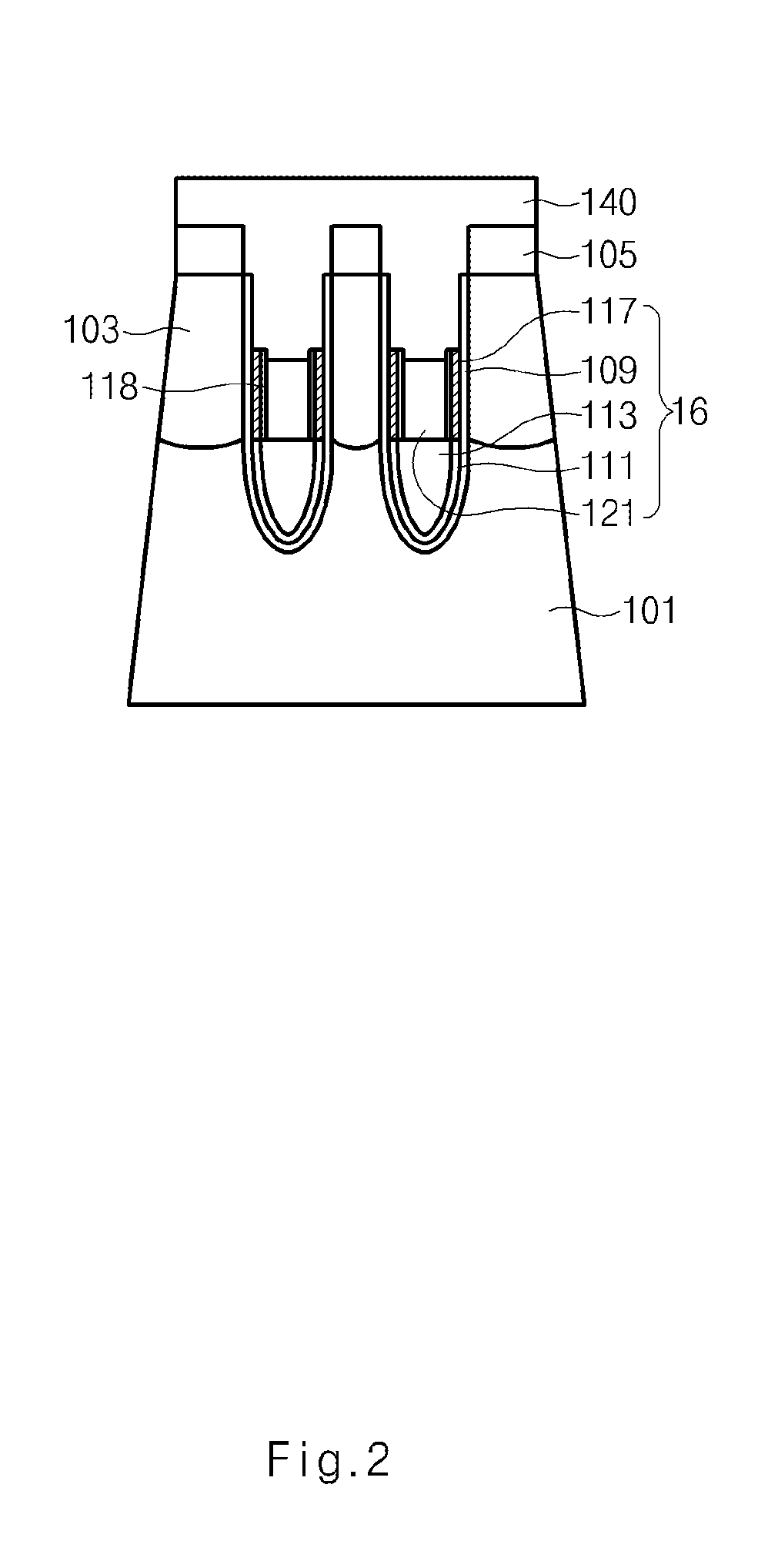
[0026]FIG. 2 is a cross-sectional view illustrating a semiconductor device according to a first exemplary embodiment of the inventive concept taken along line A-A′ of FIG. 1;

[0027]FIGS. 3A to 3H are cross-sectional views illustrating a method of fabricating a semiconductor device according to a first exemplary embodiment;

[0028]FIG. 4 is a cross-sectional view illustrating a semiconductor device according to a second exemplary embodiment of the inventive concept taken along line A-A′ of FIG. 1;

[0029]FIGS. 5A to 5E are cross-sectional views illustrat...


PUM


Abstract

A semiconductor device and a method for manufacturing the same are capable of improving GIDL in a buried gate, and preventing degradation of device characteristics and reliability due to reduction in gate resistance. The semiconductor device may include: junction regions formed at both sidewalls of a trench formed in a semiconductor substrate; a first gate electrode formed in a lower portion of the trench; a second gate electrode formed on at least one inner sidewall of the trench which overlaps one of the junction regions on the first gate electrode; and a third gate electrode formed on one side of the second gate electrode on the first gate electrode.

Description

CROSS-REFERENCE TO RELATED APPLICATION[0001]The present application claims priority to Korean patent application number 10-2012-0096486, filed on 31 Aug. 2012, which is incorporated by reference herein in its entirety.BACKGROUND[0002]1. Technical Field[0003]The inventive concept relates to a semiconductor device and a method of fabricating the same, and more particularly, to technology to improve gate-induced drain leakage (GIDL) of a buried gate and to improve device characteristic and reliability with reduction in a gate resistance.[0004]2. Related Art[0005]In recent years, although demands on large capacity of dynamic random access memories (DRAMs) have been increasing, there is a limit to increase in the capacity of the DRAMs due to increased chip size. With the increase of the chip size, the number of chips per a wafer is reduced and yield of the device is reduced. Therefore, in recent years, there are studies to reduce a cell area through change of a cell layout and thus to in...

Claims


Application Information

Patent Timeline
IPC IPC(8): H01L29/78
CPCH01L29/7831H01L29/517H01L29/78H01L29/4236H10B12/053H10B99/00H10B12/00H01L29/7813H01L21/823437H01L21/8234H01L21/283H01L21/30604H01L21/32051H01L21/32133H01L29/42364H01L29/4958H01L29/518H01L29/6653
Inventor KIM, SUNG SOO
Owner SK HYNIX INC
Why Eureka
Try Eureka