GaN-based T-type gate high-frequency device, preparation method thereof and application thereof

A high-frequency, device technology, applied in the field of GaN-based T-gate high-frequency devices and its preparation, can solve the problems of small gate length, lower mobility under the gate, and limit the speed of pattern exposure, etc., to reduce parasitic capacitance , improve frequency characteristics, and solve the effect of low production efficiency

Inactive Publication Date: 2018-09-21
SUZHOU INST OF NANO TECH & NANO BIONICS CHINESE ACEDEMY OF SCI
View PDF3 Cites 17 Cited by
  • Summary
  • Abstract
  • Description
  • Claims
  • Application Information

AI Technical Summary

Problems solved by technology

At the same time, the interface state will affect the electron mobility under the gate, which will greatly reduce the mobility under the gate and seriously affect the performance of the device. The industry also tries to avoid the etching method.
[0006] In order to obtain a smaller gate length and higher frequency characteristics, electron beam exposure technology is usually used. Although electron beam exposure technology can realize a gate length process of tens of nanometers, but because the electron beam spot is placed on the surface one by one during the exposure process For point scanning, each graphic pixel needs to stay for a certain period of time, which limits the speed of graphic exposure

Method used


Image

  • GaN-based T-type gate high-frequency device, preparation method thereof and application thereof
  • GaN-based T-type gate high-frequency device, preparation method thereof and application thereof
  • GaN-based T-type gate high-frequency device, preparation method thereof and application thereof

Examples


preparation example Construction

[0063] An embodiment of the present invention provides a method for manufacturing a GaN-based T-gate high-frequency device, including:

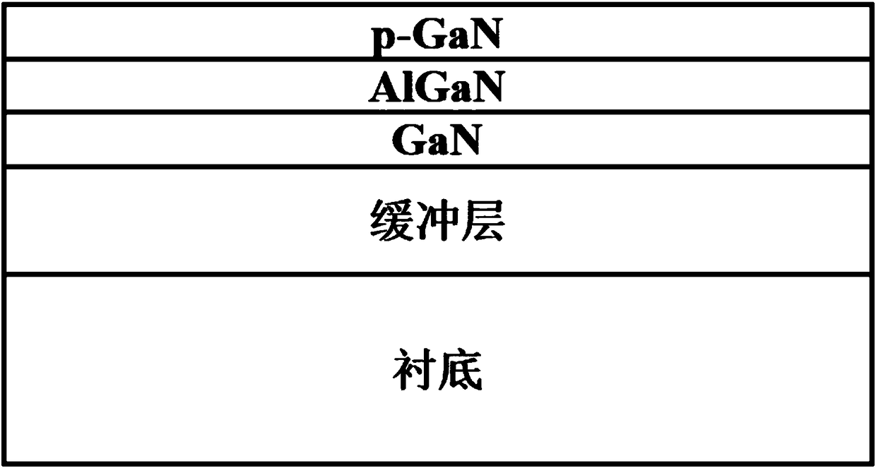
[0064] providing a heterojunction comprising a first semiconductor and a second semiconductor, the second semiconductor being formed on the first semiconductor and having a bandgap wider than that of the first semiconductor, the heterojunction having two-dimensional electrons formed therein gas;

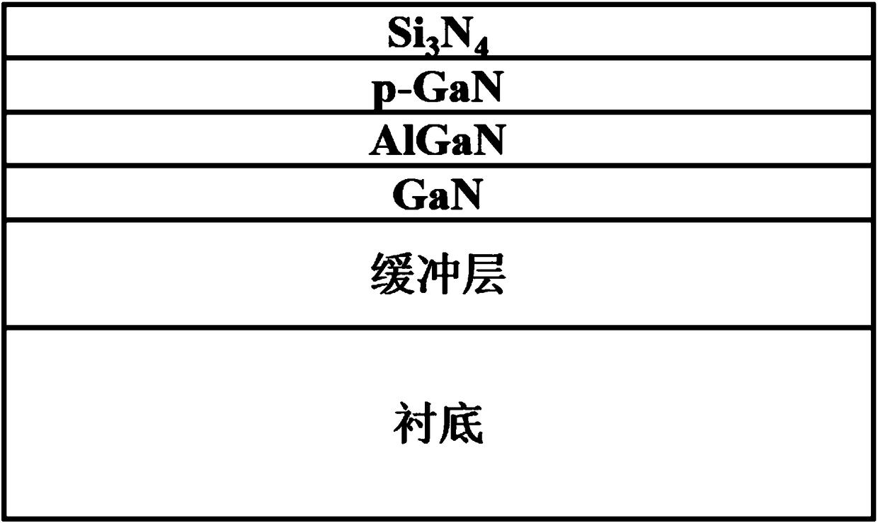
[0065] Forming a P-type semiconductor and a high-resistance semiconductor on the heterojunction, the P-type semiconductor is located in the region under the gate, and the high-resistance semiconductor is located between the P-type semiconductor and any one of the source and drain;

[0066] Make the source, drain and gate, connect the gate to the P-type semiconductor, the length of the gate is greater than the length of the P-type semiconductor, and the P-type semiconductor is used to deplete the two-dimensional electrons in the region under the gate...

Embodiment 1

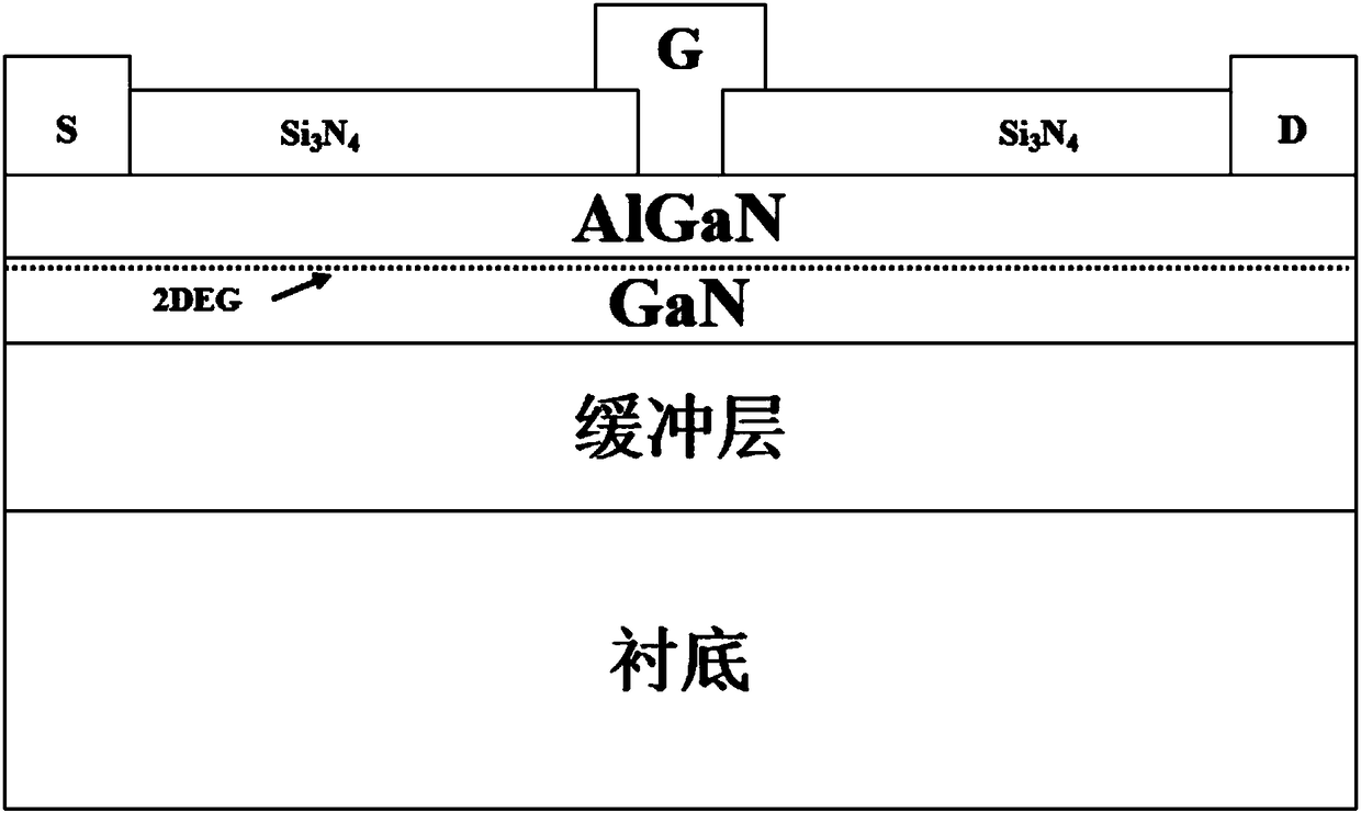
[0092] 1) Using metal organic compound chemical vapor deposition (MOCVD) to grow such as figure 2The device structure shown. The substrate material is Si, with a thickness of 200 μm to 1500 μm, preferably 400 μm; the material of the buffer layer is high resistance GaN or high resistance AlGaN, with a thickness of 1000 nm to 5000 nm, preferably 4200 nm; AlGaN / GaN heterostructure (GaN can be replaced by GaAs or other materials that can provide heterojunctions, AlGaN can be replaced by AlInN, AlGaAs or InGaAs or other materials that can provide heterojunctions) GaN thickness is 100nm to 500nm, preferably 260nm; AlGaN thickness is 15nm to 30nm, preferably 18nm, wherein the content of the Al component is 15-30wt%, preferably 18wt%; the p-type semiconductor material is p-GaN, with a thickness of 50nm-100nm, preferably 70nm;

[0093] 2) by low-pressure chemical vapor deposition (LPCVD) in the figure 2 Insulating Si deposited on the surface of the device structure shown (i.e., on ...


PUM


Abstract

The invention discloses a GaN-based T-type gate high-frequency device, a preparation method and application thereof. The GaN-based T-type gate high-frequency device includes a heterojunction includinga first semiconductor and a second semiconductor formed on the first semiconductor, a P-type semiconductor and a high-resistance semiconductor formed on a heterojunction, and a source electrode, a drain electrode and a gate, wherein the second semiconductor has a band gap wider than the first semiconductor, two-dimensional electron gas is formed in the heterojunction, the P-type semiconductor islocated in a gate lower region and is connected to the gate, the length of the gate is larger than the length of the P-type semiconductor, the P-type semiconductor is used for depleting the two-dimensional electron gas in the gate lower region, the high-resistance semiconductor is located between the P-type semiconductor and the source electrode or the drain electrode, and the source electrode andthe drain electrode can be electrically connected through the two-dimensional electronic gas. According to the GaN-based T-type gate high-frequency device, the preparation method and the applicationthereof, the etching of the gate lower region is not needed, the problems of uniformity, repeatability and damage introduced by an etching process are avoided, the electron beam exposure technology isnot needed, and the problems of low production efficiency and the like are solved.

Description

technical field [0001] The invention particularly relates to a GaN-based T-type gate high-frequency device and its preparation method and application, belonging to the technical field of semiconductor radio-frequency devices. Background technique [0002] The third-generation semiconductor material represented by gallium nitride (GaN) is after the first-generation semiconductor material represented by silicon (Si) and the second-generation semiconductor material represented by gallium arsenide (GaAs). Rapidly developed new semiconductor materials. GaN material has outstanding advantages such as large bandgap width, large electron drift velocity, high thermal conductivity, high temperature resistance and radiation resistance, and is especially suitable for making high-frequency, high-efficiency, high-temperature-resistant high-power electronic devices. Since the first GaN high electron mobility transistor was born in 1993, GaN HEMT (High Electron Mobility Transistor) devices...

Claims


Application Information

Patent Timeline
Patent Type & Authority Applications(China)
IPC IPC(8): H01L29/06H01L29/423H01L29/778H01L21/335H01L21/28
CPCH01L29/42356H01L29/0684H01L29/66462H01L29/7787
Inventor 张晓东张辉张佩佩于国浩蔡勇张宝顺
Owner SUZHOU INST OF NANO TECH & NANO BIONICS CHINESE ACEDEMY OF SCI
Why Eureka
Try Eureka