A double T-shaped gate, and a manufacturing method and an application thereof

A manufacturing method and gate foot technology, applied to electrical components, circuits, semiconductor devices, etc., can solve problems such as low yield, achieve the effects of reducing contact area, ensuring gate line width, and suppressing parasitic capacitance

Inactive Publication Date: 2018-12-28
XIAMEN SANAN INTEGRATED CIRCUIT
View PDF8 Cites 16 Cited by
  • Summary
  • Abstract
  • Description
  • Claims
  • Application Information

AI Technical Summary

Problems solved by technology

[0004] Electron beam lithography is currently an important method for fabricating nanoscale gates, because the electron beam spot size can be controlled below 2nm, and patterns smaller than 50nm can be exposed; however, the major disadvantage of electron beam lithography is that the yield is very low

Method used


Image

  • A double T-shaped gate, and a manufacturing method and an application thereof
  • A double T-shaped gate, and a manufacturing method and an application thereof
  • A double T-shaped gate, and a manufacturing method and an application thereof

Examples


Embodiment 1

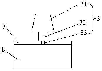
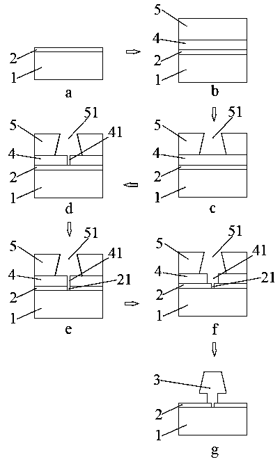
[0055] Embodiment 1: In this embodiment, the substrate 1 is preferably a gallium nitride (GaN) epitaxial wafer. refer to figure 2 The production method flowchart of middle a-f comprises the following steps: as figure 2 As shown in a, 1) GaN substrate 1 is cleaned, and silicon nitride is deposited on the GaN epitaxial wafer. In this embodiment, the thickness of deposited silicon nitride is 50nm.

[0056] Such as figure 2As shown in b, 2) Spin-coat PMMA electron beam photoresist 4 with a thickness of 350 nm on silicon nitride and bake it on a hot plate at 180°C for 2 minutes. After cooling to room temperature, continue to spin-coat Nloff5510 I-Line with a thickness of 800 nm Negative photoresist 5 was baked on a hot plate at 100°C for 2 minutes.

[0057] Such as figure 2 As shown in c, 3) Nloff5510 I-Line negative photoresist 5 exposure, the preferred energy is 1300J / m 2 , developed with 2.38% TMAH (tetramethylammonium hydroxide) at 23°C for 41 seconds. Oxygen plasma t...

Embodiment 2

[0064] Embodiment 2: In this embodiment, the substrate 1 is preferably a gallium arsenide (GaAs) epitaxial wafer. refer to figure 2 The production method flowchart of middle a-f comprises the following steps: as figure 2 As shown in a, 1) GaAs epitaxial wafer is cleaned, and silicon nitride is deposited on the GaAs epitaxial wafer. In this embodiment, the thickness of deposited silicon nitride is 50nm.

[0065] Such as figure 2 As shown in b, 2) Spin-coat PMMA electron beam photoresist 4 with a thickness of 100 nm on silicon nitride and bake it on a hot plate at 180°C for 2 minutes. After cooling to room temperature, continue to spin-coat Nloff5510 I-Line with a thickness of 600 nm Negative photoresist 5 was baked on a hot plate at 100°C for 2 minutes.

[0066] Such as figure 2 As shown in c, 3) Nloff5510 I-Line negative photoresist 5 exposure, the preferred energy is 1300J / m 2 , developed with 2.38% TMAH (tetramethylammonium hydroxide) at 23°C for 41 seconds. Oxygen...


PUM


Abstract

A double T-shaped gate, and a manufacturing method and an application thereof are provided. The double T-shaped gate comprises a gate foot, a gate root and a gate cap, wherein the gate foot and the gate root form a first level T-shaped gate, the gate root and the gate cap form a second level T-shaped gate, the gate cap is suspended, and the gate foot grows on a substrate through a dielectric passivation layer. The invention can reduce the gate resistance, and the manufacturing method thereof not only can effectively realize the small line width gate, reduce the gate parasitic capacitance, butalso can improve the efficiency of the gate fabrication.

Description

technical field [0001] The invention belongs to the field of manufacturing microelectronic devices, and in particular relates to a double T-shaped gate, a manufacturing method and an application thereof. Background technique [0002] On gallium arsenide / gallium nitride RF millimeter-wave monolithic integrated circuits, the gate length is an important parameter affecting the performance of microwave devices. Under certain conditions, the gate length is directly related to the device frequency, and reducing the gate length can greatly improve the performance of the device. frequency and gain performance. T-shaped grid is a grid shape commonly used to reduce grid resistance, such as the T-shaped grid disclosed in Chinese patent CN201611237056.4. It can be seen from the drawings that the T-shaped grid includes a grid foot and a grid cap. The feet are grown on the AlGaN / GaN epitaxial layer, and the gate cap is directly covered on the dielectric passivation layer. Another exampl...

Claims


Application Information

Patent Timeline
Patent Type & Authority Applications(China)
IPC IPC(8): H01L29/423H01L21/28H01L29/778
CPCH01L29/401H01L29/42316H01L29/778
Inventor 何先良卢青蔡文必王文平
Owner XIAMEN SANAN INTEGRATED CIRCUIT
Why Eureka
Try Eureka