

Semiconductor device and method for manufacturing the same
- Summary
- Abstract
- Description
- Claims
- Application Information
AI Technical Summary
Benefits of technology
Problems solved by technology
Method used
Image

Examples
Embodiment Construction
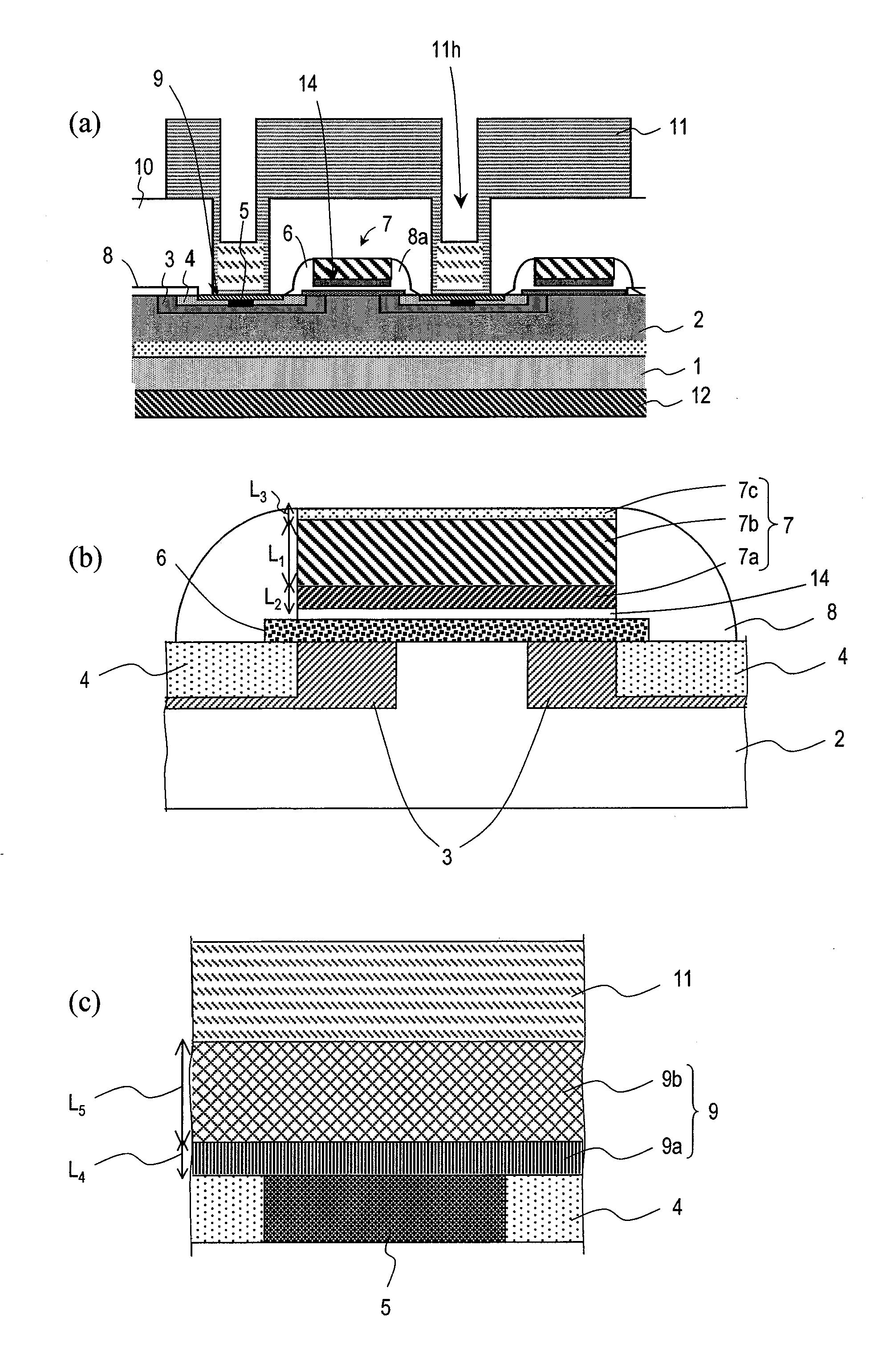
[0068]Hereinafter, embodiments of a semiconductor device according to the present invention will be described. The present invention realizes a silicon carbide semiconductor device including an ohmic electrode with no graphite formation and a low-resistance gate electrode, which is preferably usable for an insulating gate-type transistor such as a MISFET, a MOSFET or the like. In the following embodiments, the present invention will be described by way of a vertical type double implantation MISFET as an example.
[0069]FIG. 1(a) is a schematic cross-sectional view showing an embodiment of a semiconductor device according to the present invention. A structure of the semiconductor device will be briefly described.
[0070]The semiconductor device shown in FIG. 1(a) includes a silicon carbide semiconductor substrate 1 having a silicon carbide layer 2. The silicon carbide semiconductor substrate 1 is an off substrate having an off angle of 8 degrees from the (0001) surface of 4H-SiC. The sil...
PUM
 Abstract
Description
Claims
Application Information