

High speed trench DMOS
a dmos transistor, high-speed technology, applied in the direction of basic electric elements, electrical equipment, semiconductor devices, etc., can solve the problems of exacerbated problems, particularly deleterious punching at higher transistors, and the trench dmos transistor is known as punching, so as to reduce the delay of distributed rc gate propagation, low gate resistance, and low gate capacitance
- Summary
- Abstract
- Description
- Claims
- Application Information
AI Technical Summary
Benefits of technology
Problems solved by technology
Method used
Image

Examples
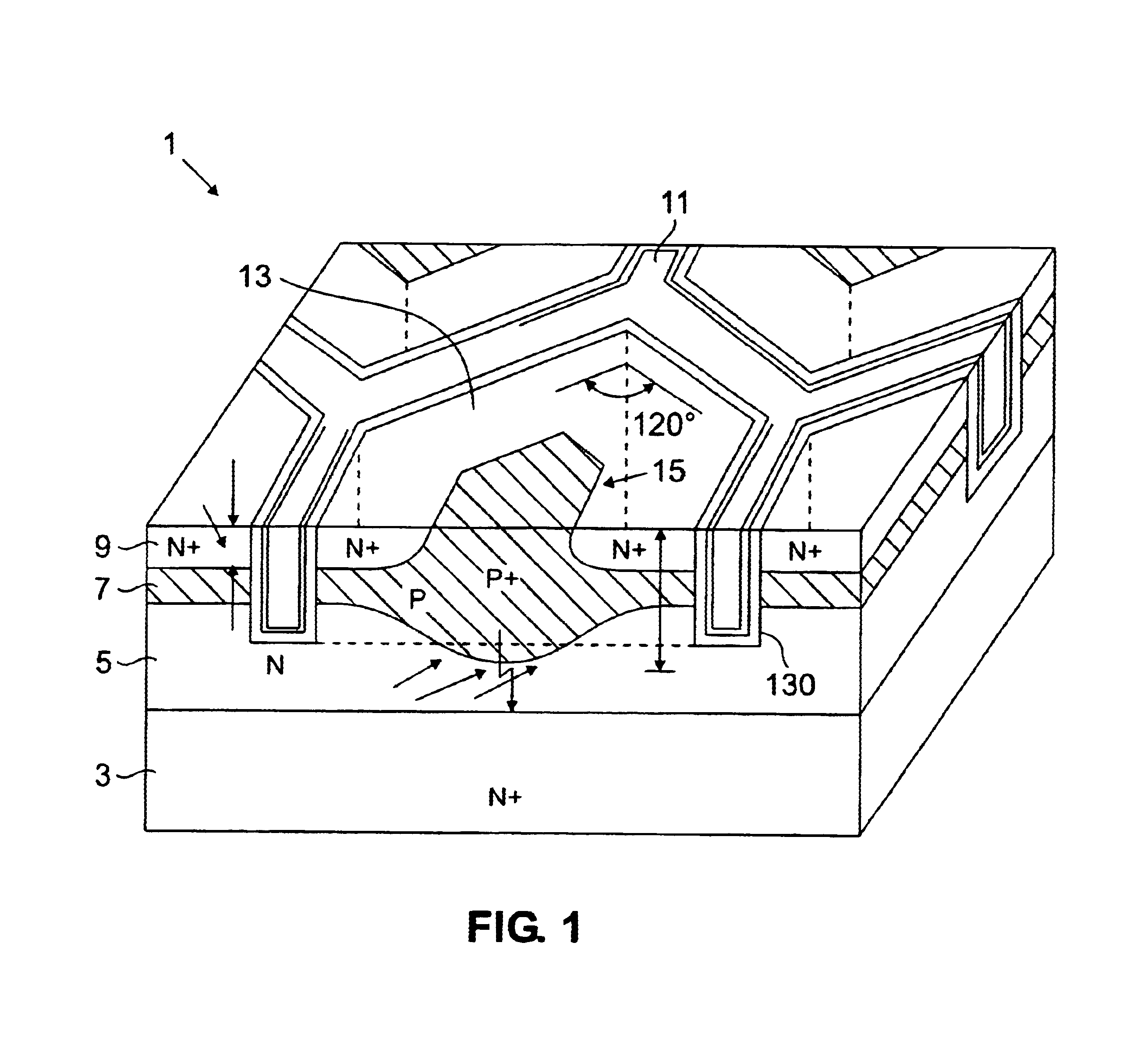
first embodiment
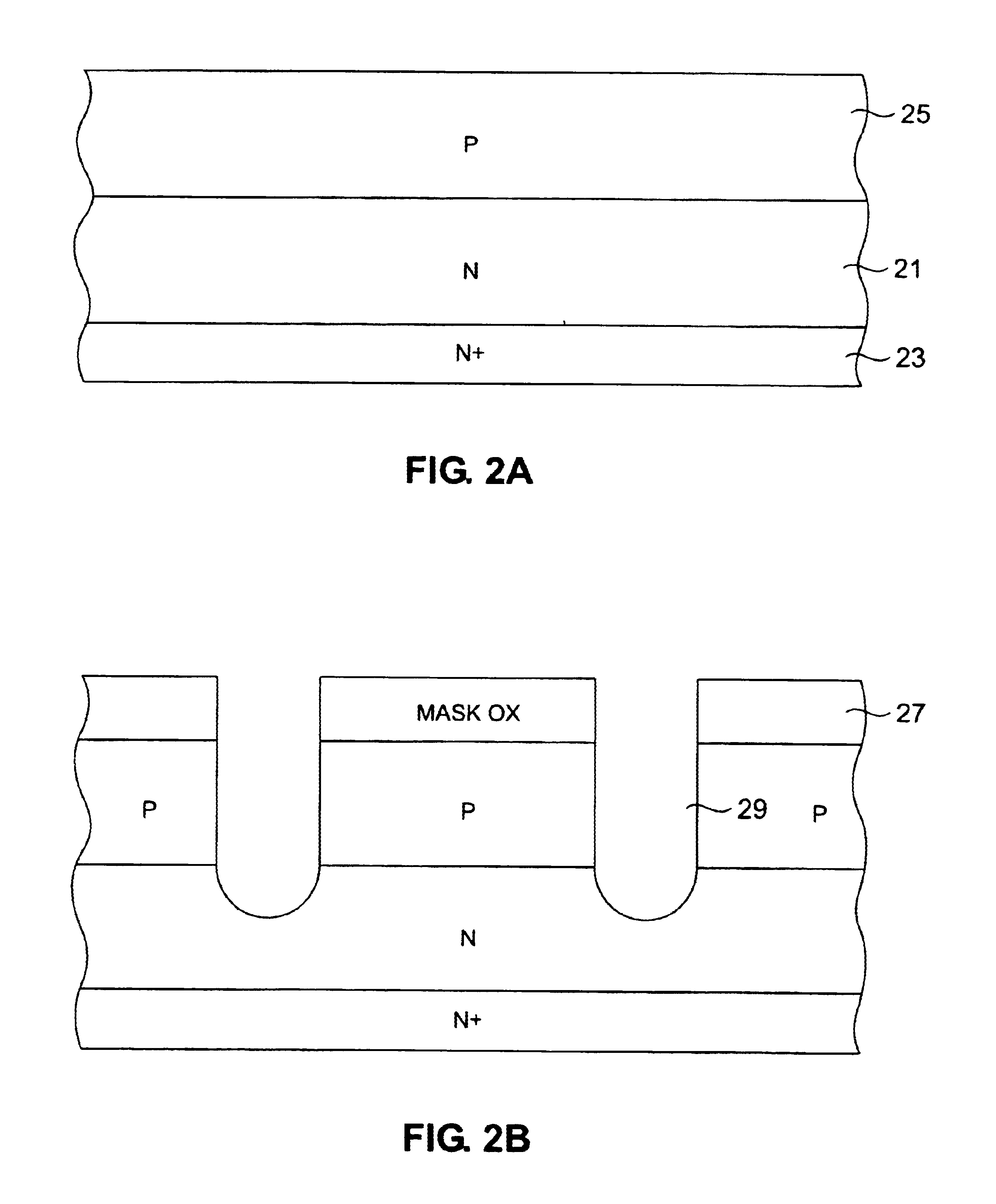
FIGS. 2A-2G shows the method of the present invention that may be used to form a DMOS device of the type depicted in FIG. 1. In FIG. 2A, an N-doped epitaxial layer 21 is grown on a conventionally N+ doped substrate 23. The epitaxial layer is typically 5.5 microns in thickness for a 30 V device. Next, P-body region 25 is formed in an implantation and diffusion step. Since the P-body implant is uniform across the substrate, no mask is needed. The P-body regions are boron implanted at 40 to 60 KEV with a dosage of 5.5×10¹³ / cm3.
In FIG. 2B, a mask oxide layer is formed by covering the surface of the epitaxial layer with an oxide layer, which is then conventionally exposed and patterned to leave mask portions 27. Mask portions 27 are used for defining the location of the trenches 29, which are dry etched through the mask openings by reactive ion etching to a depth that typically ranges from 1.5 to 2.5 microns.
In FIG. 2C, the mask portions are removed, typically by a buffer oxide etch or a...
second embodiment
FIGS. 3A-3B illustrate the method of the present invention. In this embodiment, a trench DMOS is formed substantially in accordance with the steps illustrated in FIGS. 2A-2D. However, after the deposition of the layer of polycide or refractory metal 51 over the layers of undoped polysilicon 53, doped polysilicon 55, and gate oxide 56, a polysilicon mask 57 is placed over the trench 59, and the resulting structure is subjected to etching to remove the unmasked polysilicon and polycide layers. The trench DMOS transistor is then completed in a manner similar to that depicted in FIGS. 2E-2G to yield the device depicted in FIG. 3B. In the finished device, a portion 61 of the gate layer is disposed above the source area 63, so that the distance between the drain and the portion 61 of the gate layer is greater than the distance between the drain and the source. As a result, the configuration has a lower gate resistance, especially in a shallow trench device, thereby achieving higher switch...
third embodiment
FIGS. 4A-4B illustrate the method of the present invention. In this embodiment, the trench DMOS is formed in a manner similar to that used to form the devices depicted in FIGS. 3A-3B, except that the layer of doped polysilicon 65 employed is sufficiently thick to fill the trench 67. As in the device depicted in FIGS. 3A-3B, at least a portion 69 of the gate layer in the finished device is disposed above the source area 71 so that the distance between the drain and at least a portion of the gate layer is greater than the distance between the drain and the source. This configuration, like the configuration depicted in FIGS. 3A-3B, also has a lower gate resistance, especially in a shallow trench device, and higher switching speeds.
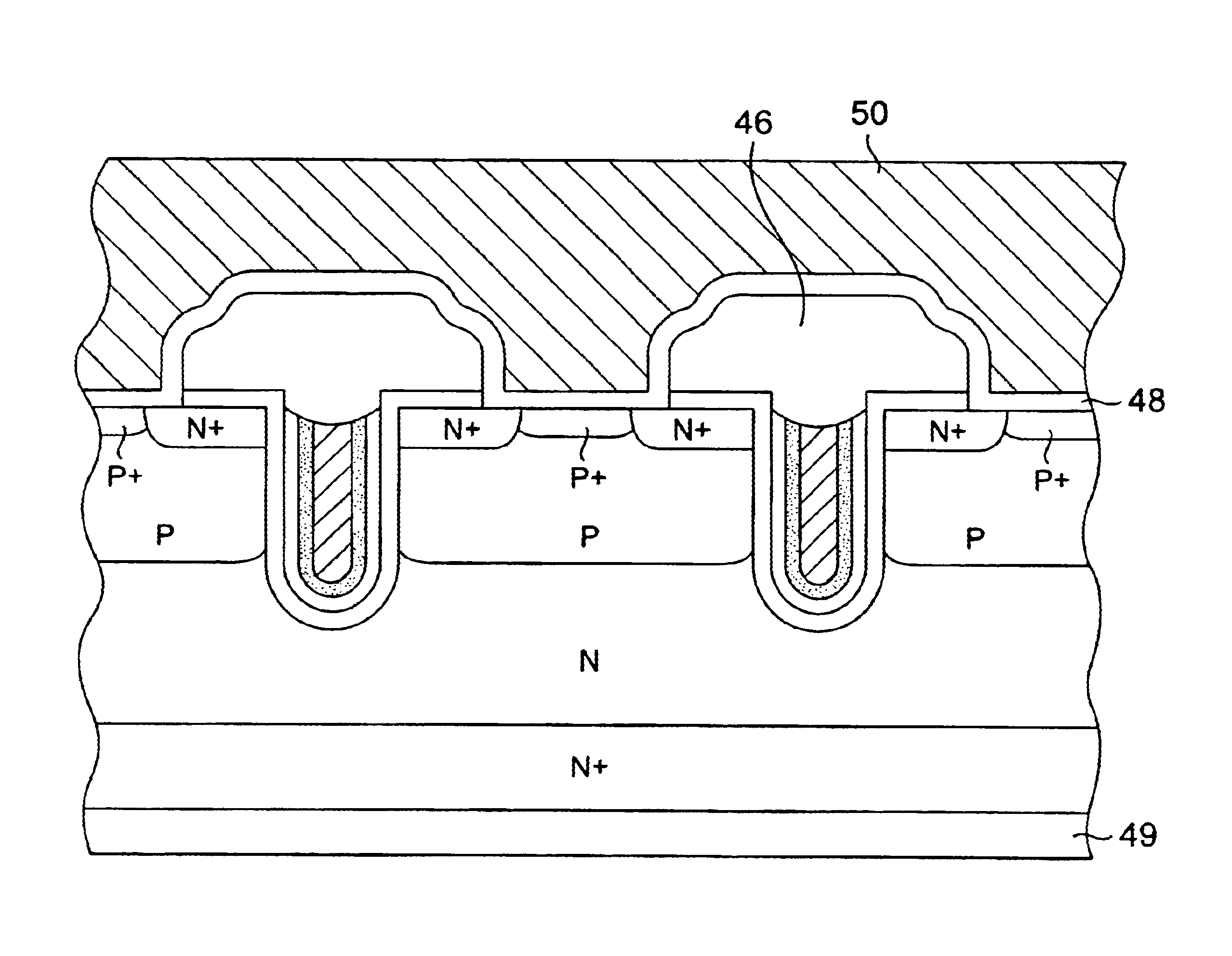
In accordance with the methodology of the present invention, the N-source region is formed after gate oxidation so that the junction depth can be controlled to very shallow depths (e.g., within the range of 0.2 to 0.5 μm), depending on the BPSG flow temperatu...
PUM
 Abstract
Description
Claims
Application Information