Trench MOSFET with terrace gate and self-aligned source trench contact

a technology of mosfet and terrace gate, which is applied in the direction of semiconductor devices, electrical devices, transistors, etc., can solve the problems of non-uniform distribution of avalanche current, on-resistance rds, and non-uniform distribution of uis (unclamp), and achieve the effect of reducing the fabrication cos

Inactive Publication Date: 2010-05-27
FORCE MOS TECH CO LTD
View PDF2 Cites 19 Cited by
  • Summary
  • Abstract
  • Description
  • Claims
  • Application Information

AI Technical Summary

Benefits of technology

[0017]Briefly, in another preferred embodiment, the trench MOSFET disclosed has the same structure with that of the first embodiment expect that, the material refilled into contact trenches is Ti / TiN / Al alloys and used as source metal layer and gate metal layer respectively as well. By employing this method, no additional front metal layer is needed for source and gate metal interconnection, and therefore reducing the fabricating cost.

Problems solved by technology

There are two technological constraints encountered by conventional trench MOSFET structure introduced above: High gate resistance Rg due to less polysilicon refilled within the gate trench when trench depth and width become shallower and narrower; and non-uniform distribution of avalanche current Iav and on-resistance Rds across wafer due to non-self-aligned source contact to trench.
Another constraint of the structure in FIG. 1 is that, there is no self-aligned source contact to trench, resulting in and a misalignment between contact and trench which will cause non-uniform distribution of UIS (Unclamp inductance Switching) current or avalanche current Iav across wafer, as well as on-resistance Rds between drain and source.
However, the terrace gate structures in prior arts do not have self-aligned source contact structure into silicon with equal space between contact trench and gate trench as shown in FIG. 6 when misalignment occurs between contact and trench masks.

Method used


Image

  • Trench MOSFET with terrace gate and self-aligned source trench contact
  • Trench MOSFET with terrace gate and self-aligned source trench contact
  • Trench MOSFET with terrace gate and self-aligned source trench contact

Examples


Embodiment Construction

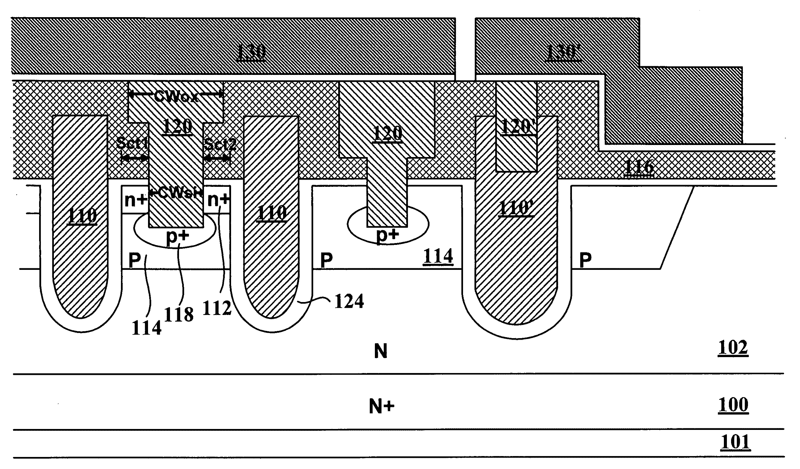
[0029]Briefly, in a preferred embodiment, as shown in FIG. 5, the present invention disclosed a trench MOSFET element formed on a substrate 100. Onto the said substrate 100, grown a first semiconductor type epitaxial layer 102 formed by a first semiconductor type silicon layer. The MOSFET element further includes a plurality of trenches filled up polysilicon to form a plurality of narrow trench gates 110 and at least a wide trench gate 110′ which is wider than the trenches 110 for gate connection. Each trench is covered with a gate insulation layer 124 on the inner surface thereof, and to fill these trenches, doped poly was deposited not within those trenches but to form terrace gates, the narrow trench gates 110 and at least a wide trench gate 110′, above the gate insulation layer 124. On the first semiconductor type epitaxial layer 102, a plurality of body regions 114 are formed by a second semiconductor type silicon layer, which are extending between the said trench gates, the na...


PUM


Abstract

A trench MOSFET with terrace gate is disclosed for self-aligned contact. When refilling the gate trenches, the deposited polysilicon layer is higher than the sidewalls of the trenches to be used as a terrace gate of the MOSFET. The source contact width is determined by mesa width between two adjacent trenches minus 2 times of the oxide thickness deposited on the mesa instead of contact mask width which is wider than silicon contact width. Therefore, the position of source contact is still unchanged even if the misalignment of trench mask happens. At the same time, by using terrace gates, the Rg is thus reduced because the terrace gate provides more polysilicon as gate material than the conventional trench gate.

Description

BACKGROUND OF THE INVENTION[0001]1. Field of the Invention[0002]This invention relates generally to the cell configuration and fabrication process of trench MOSFET devices. More particularly, this invention relates to a novel and improved cell structure and improved process of fabricating a trench MOSFET with terrace gate for self-aligned source contact.[0003]2. The Prior Arts[0004]Please refer to FIG. 1 for a conventional structure of MOSFET. The trench MOSFET is formed on an N+ substrate 900 on which an N doped epitaxial layer 902 is grown. Inside said epitaxial layer 902, a plurality of trenches 910a are etched and filled with N+ doped poly within trenches to serve as trench gates 910 over an insulating layer 908. Between each trench, there is a P-body region 912 introduced by Ion Implantation, and n+ source regions 914 near the top surface of said P-body area. Said source regions are connected to source metal 920 via source contact trench 916 through a layer of insulator 918. Sa...

Claims


Application Information

Patent Timeline
Patent Type & Authority Applications(United States)
IPC IPC(8): H01L27/088H01L21/8234
CPCH01L21/823437H01L21/823487H01L27/088H01L29/41741H01L29/7823H01L29/4236H01L29/456H01L29/66734H01L29/7813H01L29/41766
Inventor HSIEH, FU-YUAN
Owner FORCE MOS TECH CO LTD
Why Eureka
Try Eureka