Semiconductor device and method for fabricating the same

a technology of semiconductor devices and sinkers, which is applied in the direction of semiconductor devices, basic electric elements, electrical appliances, etc., can solve the problems of affecting the performance of the device, the p+ polysilicon process is not mature, and the device is difficult to shrink the area, so as to reduce the lateral size of the occupied area, improve the device performance, and reduce the resistance

Active Publication Date: 2014-02-20
SHANGHAI HUAHONG GRACE SEMICON MFG CORP
View PDF5 Cites 19 Cited by
  • Summary
  • Abstract
  • Description
  • Claims
  • Application Information

AI Technical Summary

Benefits of technology

[0059]Substitution of the P+ sinker of the conventional RF LDMOS device for the metal plug can reduce a lateral size of the occupied area and hence leads to resistance reduction and an improvement of device performance. Moreover, deposition of filler metal onto the gate of the device can result in the reduction of gate resistance. In addition, as formation of the filler metal on the gate is well compatible with the process of forming the metal plug, no additional cost will be introduced.

Problems solved by technology

For example, one deficiency is that lateral diffusion of the P+sinker increases difficulty in shrinking the area of the device, and another deficiency is that the P+ sinker has a high resistance which affects the performance of the device, especially its working frequency.
However, it still has two drawbacks as follows: first, due to limitations in process control, the P+ polysilicon process is not mature and has not been widely used; and secondly, the lateral diffusion issue still exists and the sinker resistance is still much higher than a metal resistance.

Method used


Image

  • Semiconductor device and method for fabricating the same
  • Semiconductor device and method for fabricating the same
  • Semiconductor device and method for fabricating the same

Examples


embodiment 1

[0079]In this embodiment, a semiconductor device embodying the present invention may be fabricated using a method including the steps discussed in detail below.

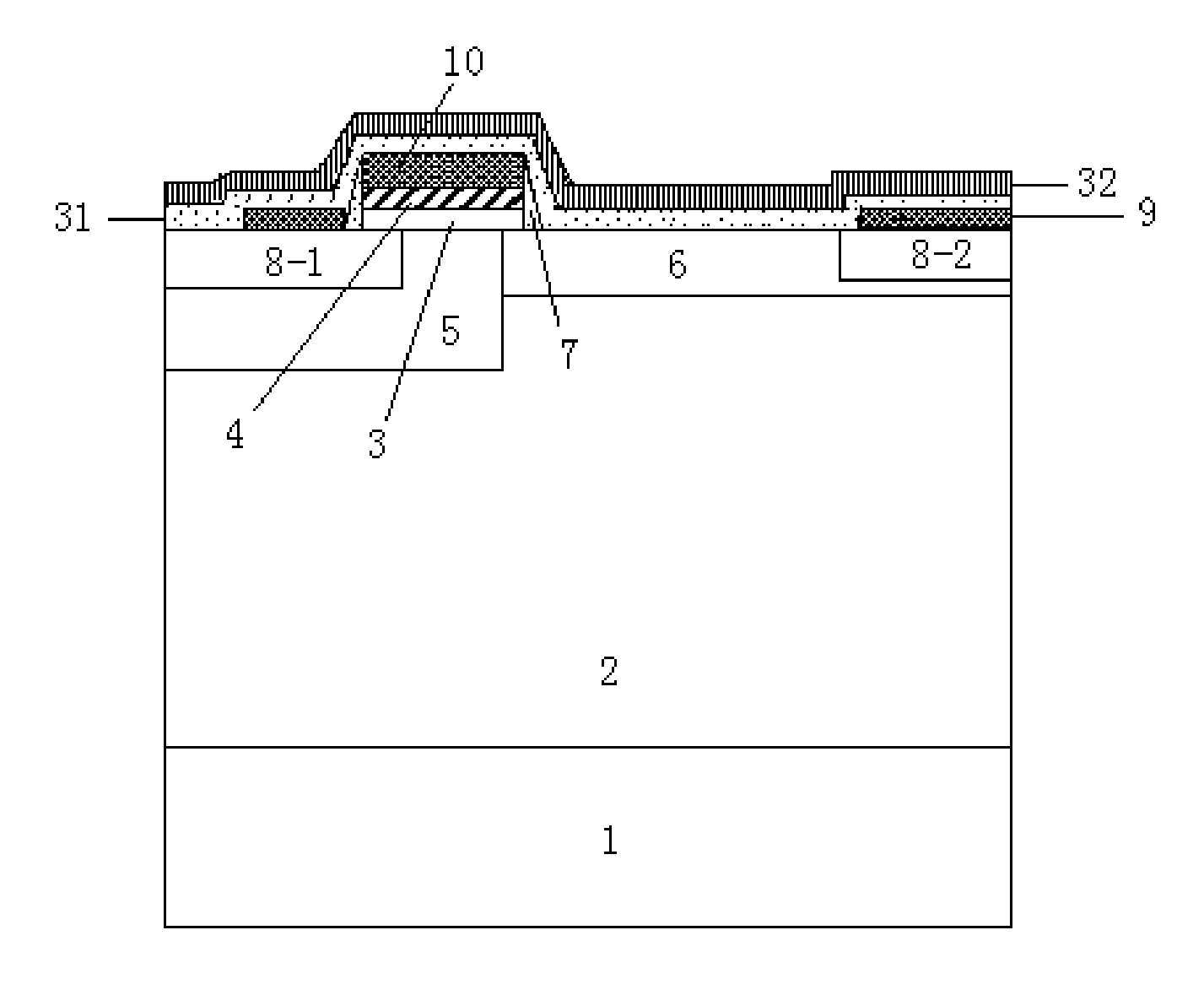
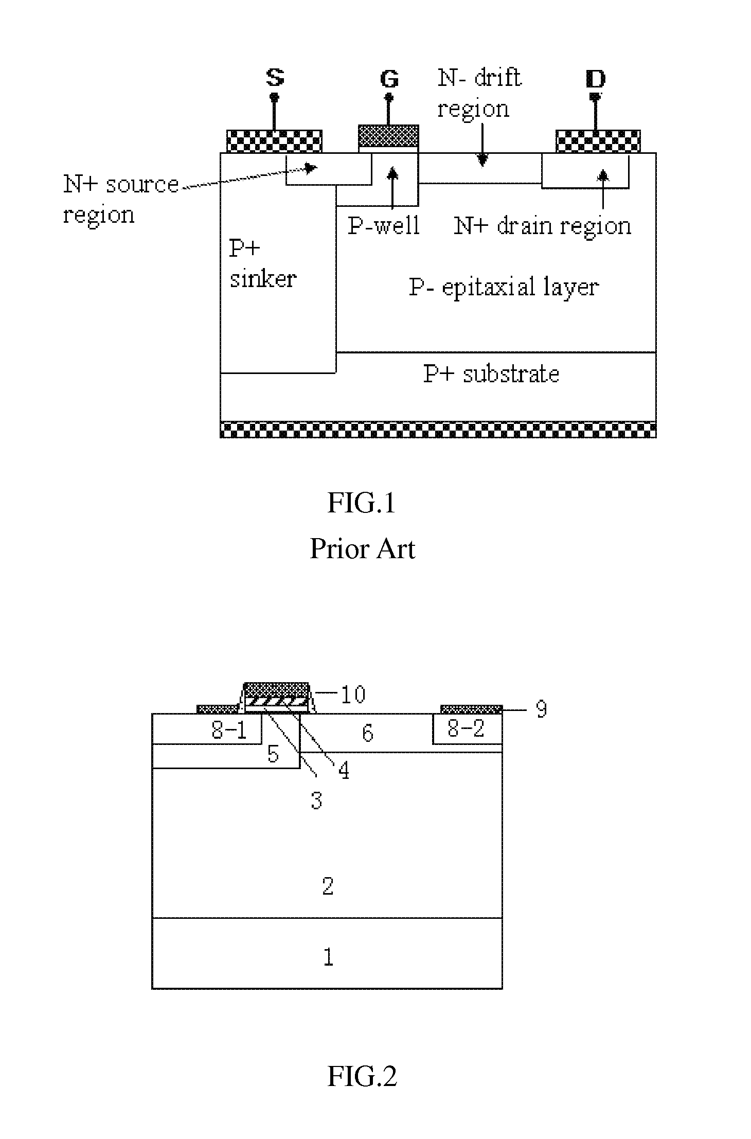
[0080]Turning now to FIG. 2, in a first step of the method, a P− epitaxial layer 2 is formed over a P+ substrate 1 (which is typically doped with boron and has a resistivity of 0.01 Ω·cm to 0.02 Ω·cm). Thickness and doping concentration of the epitaxial layer may be determined by the designed voltage endurance of the semiconductor device being fabricated. For example, a P− epitaxial layer 2 with a resistivity of 10 Ω·cm to 20 Ω·cm and a thickness of 5 μm to 8 μm may be formed to achieve a voltage endurance of 60 V for the device. Next, a gate silicon oxide film 3 having a thickness of, for example, 150 Å to 1000 Å, is deposited over the P-epitaxial layer 2. Moreover, a polysilicon film with a thickness of 1000 Å to 6000 Å is deposited over the gate silicon oxide film 3. Thereafter, a polysilicon gate 4 is formed by a photolit...

embodiment 2

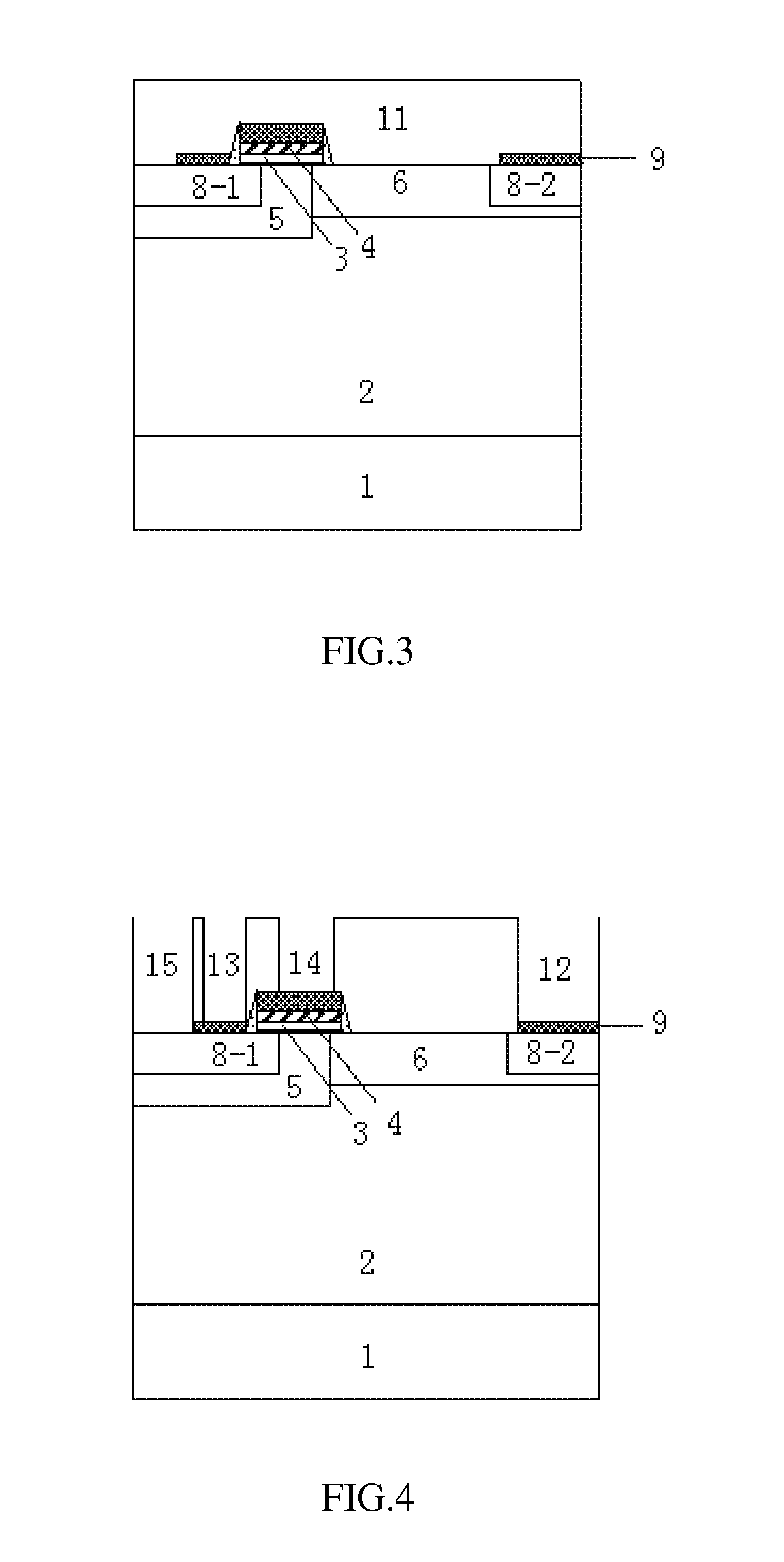
[0089]This embodiment provides a method that differs from the method of Embodiment 1 only in that, in the fourth step, with reference to FIG. 5a, photoresist 15-1 is first coated on the top face of the intermediate dielectric layer 11, filling the drain contact hole 12, the source contact hole 13 and the gate trench 14; next, the deep trench 151 is formed by etching a portion of the P− epitaxial layer 2 exposed in the dielectric trench 15 while the holes and trenches other than the dielectric trench 15 is being protected; and thereafter, P-type ions are implanted into side faces of the deep trench 151 by tilted implantation with an ion concentration of 5E17 cm−3 to 5E19 cm−3. This method can lead to further reduction of the contact resistance between the P-type material and the filler metal and hence an improvement of the performance of the resulting device.

embodiment 3

[0090]This embodiment provides a method that differs from the method of Embodiment 1 only in that, in the third step, only the drain contact hole 12, the source contact hole 13 and the gate trench 14 are formed, and that in the fourth step, a metal plug area is first opened by photolithography to define the dielectric trench 15 while the drain contact hole 12, the source contact hole 13 and the gate trench 14 are being protected by the photoresist 15-1, and then the dielectric trench 15 and the deep trench 151 are formed by etching the intermediate dielectric layer 11 and the P− epitaxial layer 2.

Embodiment 4

[0091]This embodiment provides a method that differs from the method of Embodiment 1 only in that, in the third step, only the drain contact hole 12 and the source contact hole 13 are formed, and that in the fourth step, an area above the polysilicon gate 4 and a metal plug area are first opened by photolithography to define the gate trench 14 and the dielectric trench 15, respe...


PUM

PropertyMeasurementUnit
thicknessaaaaaaaaaa
voltage enduranceaaaaaaaaaa
resistivityaaaaaaaaaa

Abstract

A semiconductor device includes: a P+ substrate; a P− epitaxial layer over the P+ substrate; a P-well and an N− drift region in the P− epitaxial layer and laterally adjacent to each other; an N+ source region in the P-well and connected to a front-side metal via a first contact electrode; an N+ drain region in the N− drift region and connected to the front-side metal via a second contact electrode; a gate structure on the P− epitaxial layer and connected to the front-side metal via a third contact electrode; and a metal plug through the P− epitaxial layer and having one end in contact with the P+ substrate and the other end connected to the front-side metal, the metal plug being adjacent to one side of the N+ source region that is farther from the N− drift region. A method for fabricating the semiconductor device is also disclosed.

Description

CROSS-REFERENCES TO RELATED APPLICATIONS[0001]This application claims the priority of Chinese patent application number 201210295845.9, filed on Aug. 17, 2012, the entire contents of which are incorporated herein by reference.TECHNICAL FIELD[0002]The present invention relates to a semiconductor device and a method for fabricating the semiconductor device.BACKGROUND[0003]Radio frequency (RF) laterally diffused metal oxide semiconductor (LDMOS) device has gained high mark acceptance. In particular, with the increasingly wide applications of the telecommunications technology, RF LDMOS device, as a new kind of power device, will get more and more attentions.[0004]FIG. 1 depicts the fundamental structure of a conventional RF LDMOS device. It typically includes a heavily doped P-type substrate (with a resistivity of 0.01 Ω·cm to 0.02 Ω·cm). A P-type epitaxial layer is grown on the P-type substrate. The thickness and doping concentration of the P-type epitaxial layer are determined by the ...

Claims


Application Information

Patent Timeline
Patent Type & Authority Applications(United States)
IPC IPC(8): H01L29/78H01L29/66
CPCH01L29/66681H01L29/7816H01L29/402H01L29/4175H01L29/41766H01L29/456H01L29/4933H01L29/665H01L29/66659H01L29/7835
Inventor XIAO, SHENGAN
Owner SHANGHAI HUAHONG GRACE SEMICON MFG CORP
Why Eureka
Try Eureka