Display device and electronic device
a display device and electronic technology, applied in the field of display devices, can solve the problems of low reliability of conventional display devices and the possibility of malfunction, and achieve the effect of suppressing the increase in the size of the frame of the display device and improving the reliability of the display devi
- Summary
- Abstract
- Description
- Claims
- Application Information
AI Technical Summary
Benefits of technology
Problems solved by technology
Method used
Image

Examples
embodiment 1
[0034]In this embodiment, an example of a display device which is one embodiment of the present invention will be described.
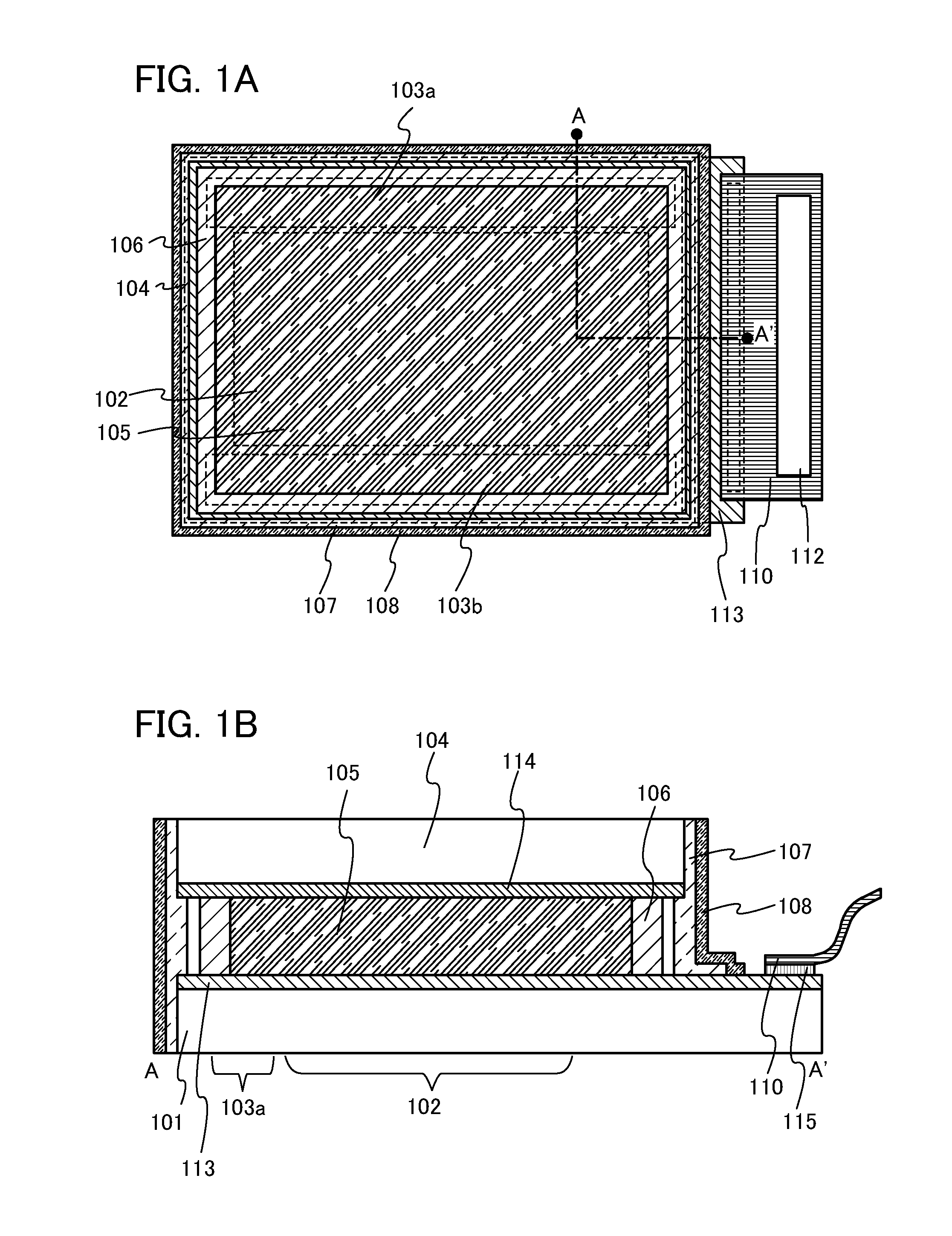
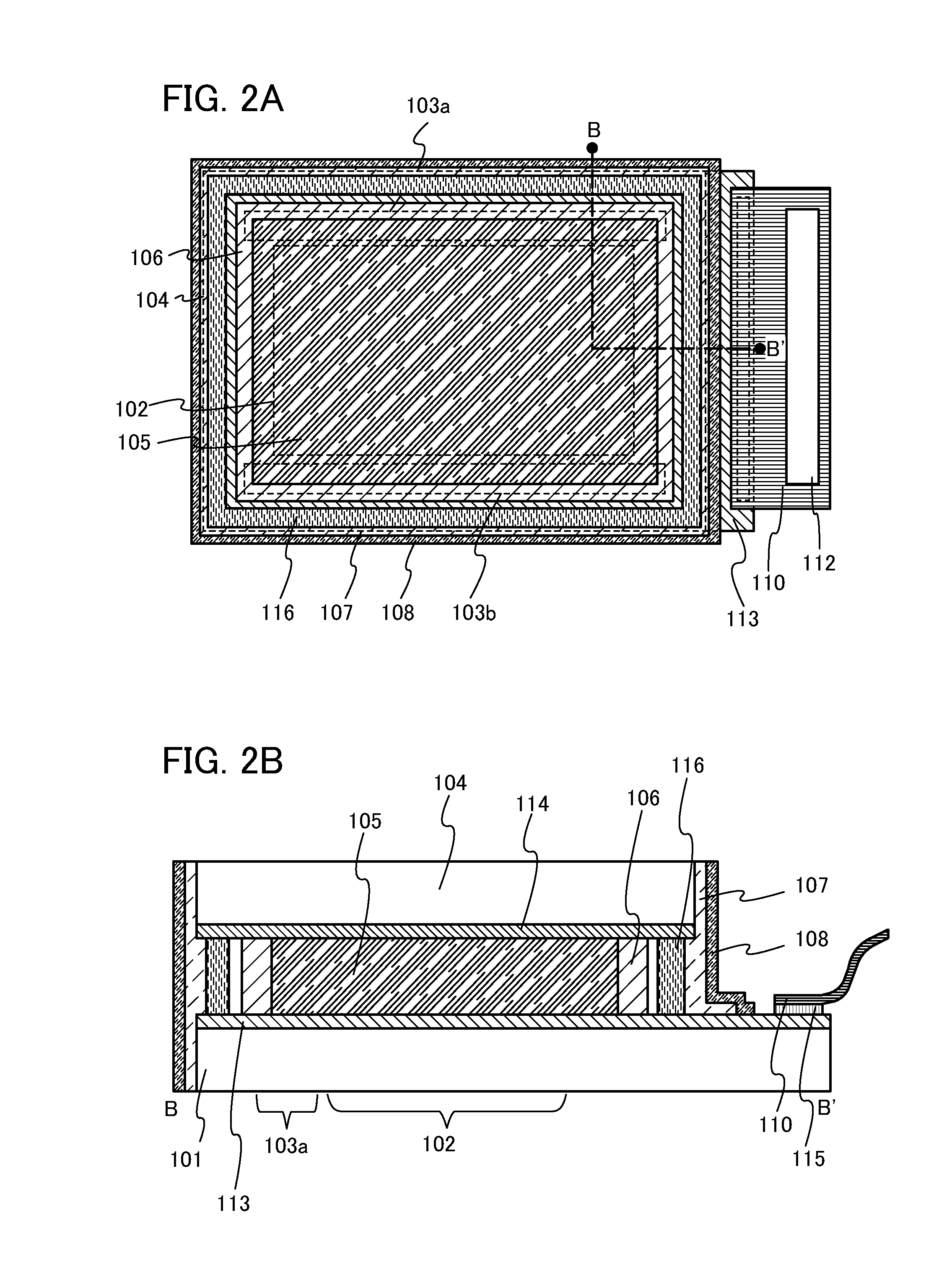
[0035]A structural example of the display device according to this embodiment will be described with reference to FIGS. 1A and 1B.
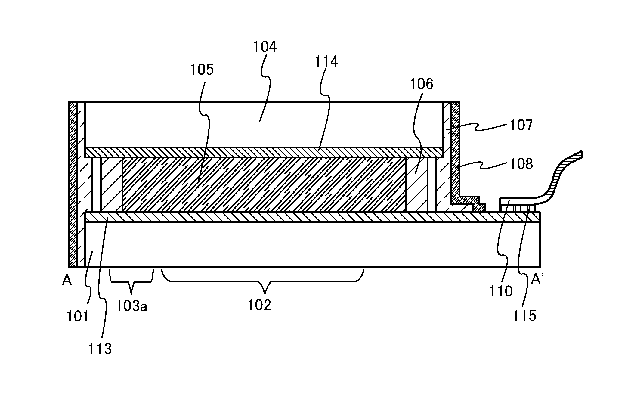
[0036]FIG. 1A is a schematic top view of the display device, and FIG. 1B is a schematic cross-sectional view along line A-A′ in FIG. 1A. Note that for convenience, some of the components of the display device are not shown in FIG. 1A.
[0037]The display device illustrated in FIGS. 1A and 1B includes a substrate 101, a substrate 104, a liquid crystal layer 105 included in a display element, a sealant 106, a sealant 107, and a sealant 108.
[0038]The substrate 101 is provided with a layer 113 in which an element such as a transistor for controlling an electric field of the liquid crystal layer 105 is formed. Note that the layer 113 also includes an insulating layer having a function as a protective layer, a planarization layer, or the like...
embodiment 2
[0122]In this embodiment, an example of a liquid crystal display device including a transistor in which a metal oxide semiconductor is used for a channel formation region will be described as an example of the display device.
[0123]Examples of display methods of the liquid crystal display device according to this embodiment include a TN (twisted nematic) mode, an IPS (in-plane switching) mode, a STN (super twisted nematic) mode, a VA (vertical alignment) mode, an ASM (axially symmetric aligned micro-cell) mode, an OCB (optically compensated birefringence) mode, an FLC (ferroelectric liquid crystal) mode, an AFLC (antiferroelectric liquid crystal) mode, an MVA (multi-domain vertical alignment) mode, a PVA (patterned vertical alignment) mode, an FFS (fringe field switching) mode, a TBA (transverse bend alignment) mode, and the like.
[0124]A liquid crystal element may be formed using a liquid crystal composition including a liquid crystal exhibiting a blue phase and a chiral material. Th...
embodiment 3
[0216]In this embodiment, examples of electronic devices each provided with a panel including a display device are described with reference to FIGS. 13A to 13D.
[0217]An electronic device in FIG. 13A is an example of a portable information terminal.
[0218]The electronic device illustrated in FIG. 13A includes a housing 1011 which is provided with a panel 1012, a button 1013, and a speaker 1014.
[0219]Note that the housing 1011 may be provided with a connection terminal for connecting the electronic device to an external device and a button for operating the electronic device.
[0220]The panel 1012 may be formed using the display device in Embodiment 1 or 2.
[0221]The panel 1012 may be a touch panel, in which case touch detection can be performed on the panel 1012. As the touch panel, an optical touch panel, a capacitive touch panel, a resistive touch panel, or the like can be used, for example.
[0222]The button 1013 is provided on the housing 1011. When the button 1013 is a power button, f...
PUM
 Abstract
Description
Claims
Application Information
 - R&D
- Intellectual Property
- Life Sciences
- Materials
- Tech Scout
- Unparalleled Data Quality
- Higher Quality Content
- 60% Fewer Hallucinations
Browse by: Latest US Patents, China's latest patents, Technical Efficacy Thesaurus, Application Domain, Technology Topic, Popular Technical Reports.
© 2025 PatSnap. All rights reserved.Legal|Privacy policy|Modern Slavery Act Transparency Statement|Sitemap|About US| Contact US: help@patsnap.com