Semiconductor memory device

a memory device and semiconductor technology, applied in the field of semiconductor memory devices, can solve the problems of invalid data being written or read, invalid data being written or written, and address access time taa may be lost or lost,

Active Publication Date: 2014-03-06
SK HYNIX INC
View PDF13 Cites 18 Cited by
  • Summary
  • Abstract
  • Description
  • Claims
  • Application Information

AI Technical Summary

Benefits of technology

[0026]In a write operation a generation timing of a column selection signal is adjusted corresponding to the arrangement locations of a plurality of unit memory regions, and in a read operation, a generation timing of a read enable signal is adjusted corresponding to the arrangement locations of the plurality of unit memory regions, so that it is possible to write and read valid data.
[0027]Furthermore, since a RC delay is used as a delay factor required when the generation timings of the column selection signal and the read enable signal, even when a PVT variation has occurred, it is possible to generate the column selection signal and the read enable signal at a desired timing.

Problems solved by technology

In such a case, since the column selection signal YI_S is generated later or earlier than a transmission time point of write data based on the arrangement location of the unit memory region, a write recovery time tWR may be lost or invalid data may be written.
In such a case, an address access time tAA may be lost or invalid data may be read.
As a consequence, due to the PVT variation, invalid data may be written or read.

Method used


Image

  • Semiconductor memory device
  • Semiconductor memory device
  • Semiconductor memory device

Examples


Embodiment Construction

[0038]Exemplary embodiments of the present invention will be described below in more detail with reference to the accompanying drawings. The present invention may, however, be embodied in different forms and should not be construed as limited to the embodiments set forth herein. Rather, these embodiments are provided so that this disclosure will be thorough and complete, and will fully convey the scope of the present invention to those skilled in the art. Throughout the disclosure, like reference numerals refer to like parts throughout the various figures and embodiments of the present invention.

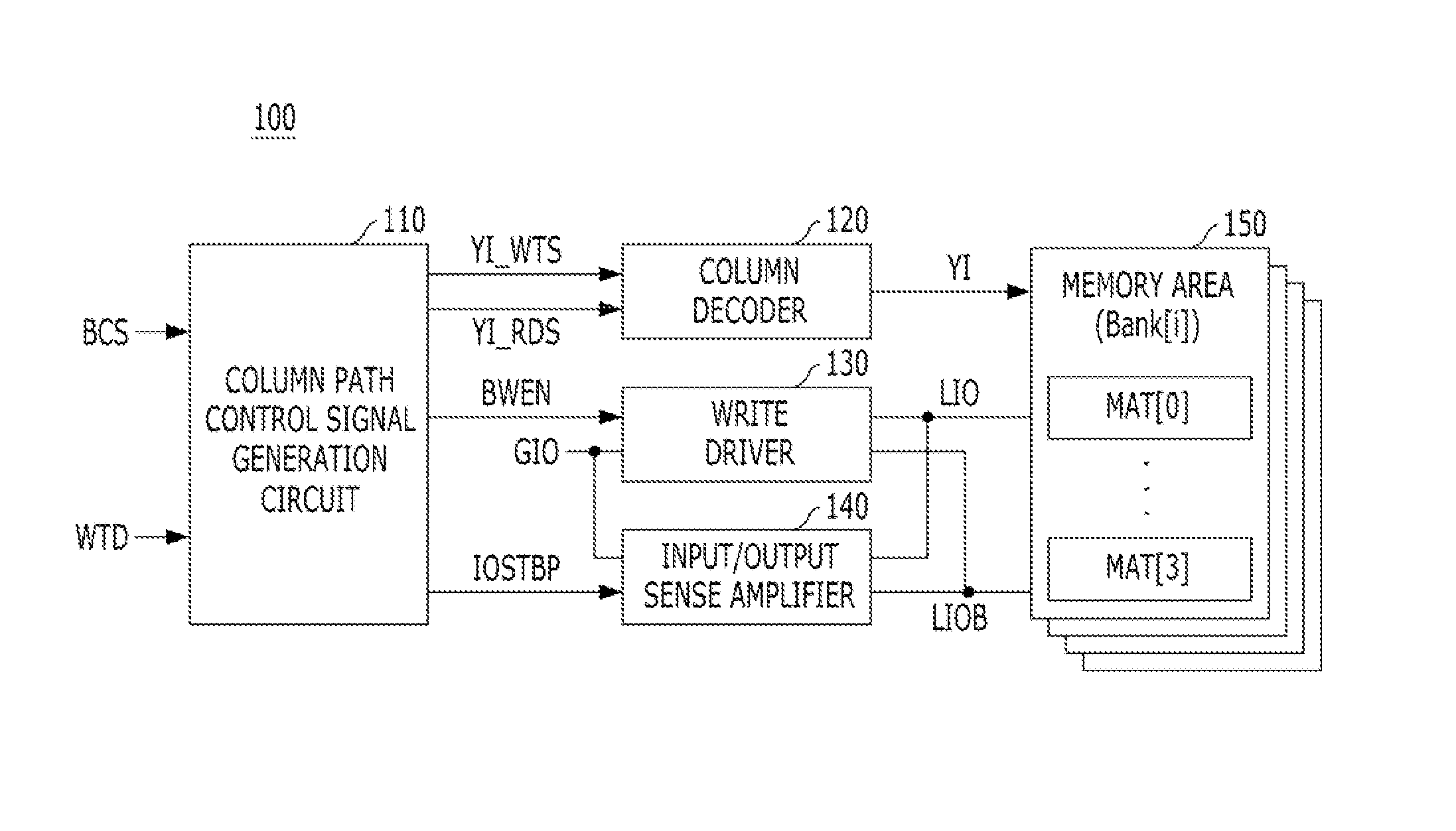
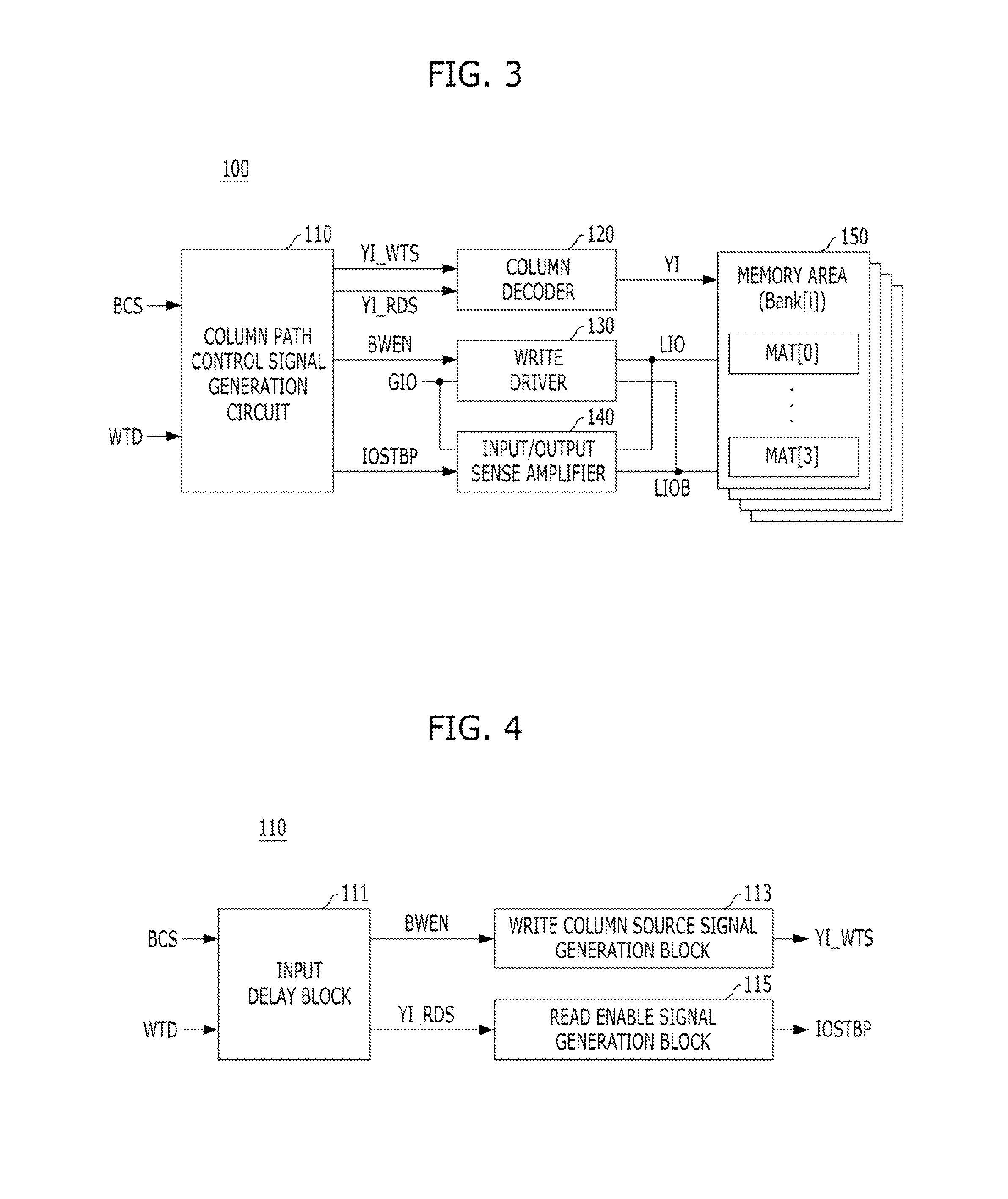
[0039]FIG. 3 is a block diagram illustrating a semiconductor device in accordance with an embodiment of the present invention.

[0040]Referring to FIG. 3, a semiconductor device 100 includes a column path control signal generation circuit 110, a column decoder 120, a write driver (WD) 130, an input / output sense amplifier (IOSA) 140, and a memory area 150. The column path control signal generat...


PUM


Abstract

A semiconductor memory device includes a first signal generation unit configured to sequentially generate first and second delay signals in response to a first column control signal, the first and second delay signals having reflected a delay time and a multiplied delay time selected from a plurality of delay times in correspondence with an arrangement location of a unit memory region, through data is input/output, respectively, and a second signal generation unit configured to generate a second column control signal delayed by the selected delay time as compared with the first column control signal, to determine an activation time point of the second column control signal in response to the first delay signal, and to determine a deactivation time point of the second column control signal in response to the second delay signal.

Description

CROSS-REFERENCE TO RELATED APPLICATIONS[0001]The present application claims priority of Korean Patent Application No. 10-2012-0094440, filed on Aug. 28, 2012, which is incorporated herein by reference in its entirety.BACKGROUND[0002]1. Field[0003]Exemplary embodiments of the present invention relate to a semiconductor design technology, and more particularly, to a semiconductor memory device.[0004]2. Description of the Related Art[0005]In general, a semiconductor memory device such as a dynamic random access memory (DRAM) performs a write operation to store data or a read operation to read stored data.[0006]The write operation may be performed in a stater in which a word line (WL) has been activated by an active command. In the write operation, data loaded on a global input / output line GIO is transferred to a local data input / output line (LIO) by a write driver (WD), the data loaded on the local input / output line (LIO) is transferred to a bit line (BL) selected based on a column sel...

Claims


Application Information

Patent Timeline
Patent Type & Authority Applications(United States)
IPC IPC(8): G11C7/22G11C7/10
CPCG11C7/1087G11C7/227G11C11/4076G11C11/4097G11C2207/005G11C2207/229G11C7/10G11C7/22G11C7/06G11C7/12G11C8/10
Inventor PARK, HEAT-BIT
Owner SK HYNIX INC
Why Eureka
Try Eureka