Optoelectric device with semiconductor microwires or nanowires and method for manufacturing the same

Active Publication Date: 2014-03-20
ALEDIA +1
View PDF2 Cites 25 Cited by
  • Summary
  • Abstract
  • Description
  • Claims
  • Application Information

AI Technical Summary

Benefits of technology

[0010]Another aspect of an embodiment of the present invention is to accurately and uniformly control the position, the geometry, and the crystallographic properties of each microwire or na

Problems solved by technology

A disadvantage of the method described in document U.S. Pat. No. 7,829,443 is that nanowires first develop from the substrate in the opening

Method used


Image

  • Optoelectric device with semiconductor microwires or nanowires and method for manufacturing the same
  • Optoelectric device with semiconductor microwires or nanowires and method for manufacturing the same
  • Optoelectric device with semiconductor microwires or nanowires and method for manufacturing the same

Examples


Example

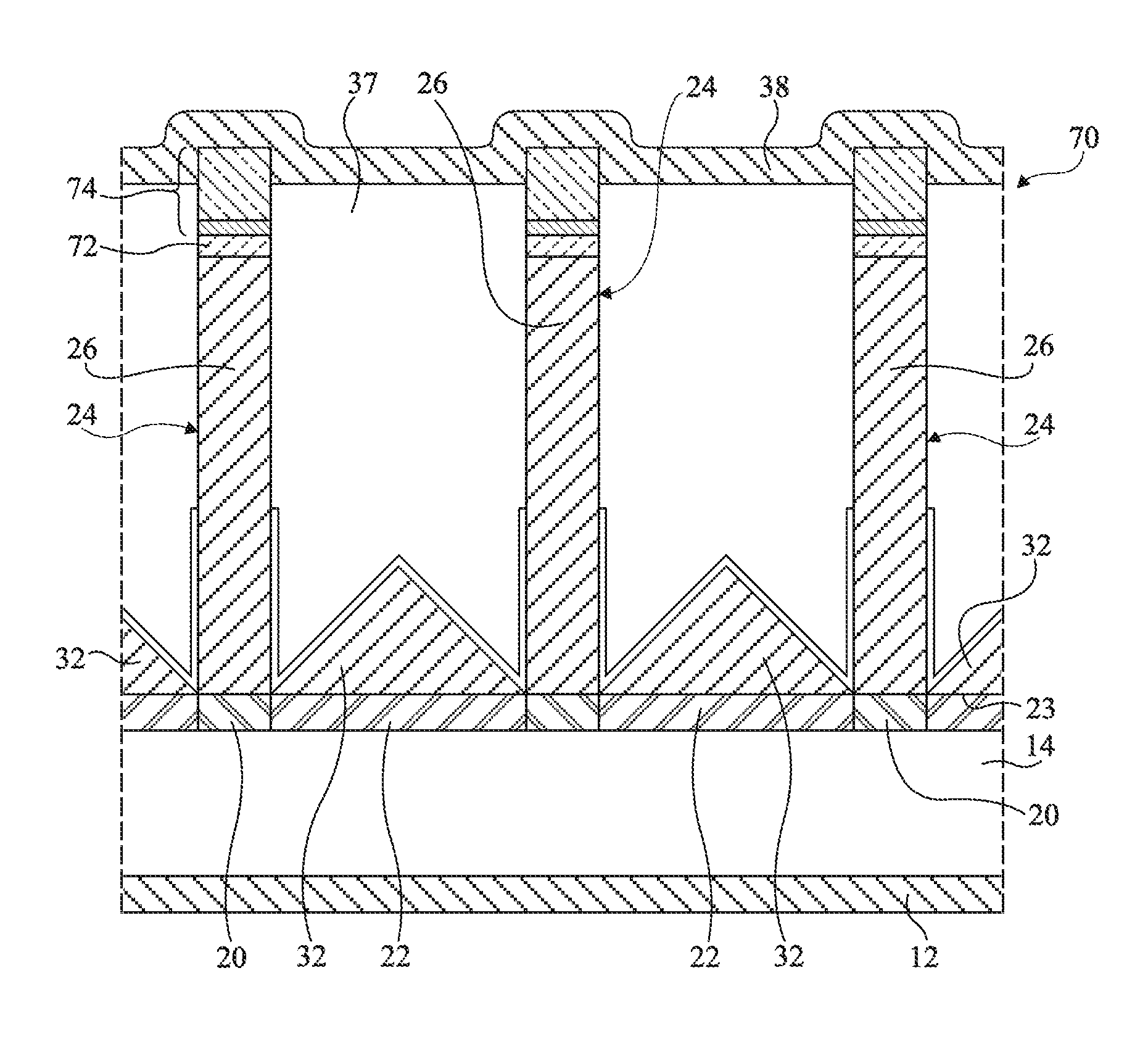
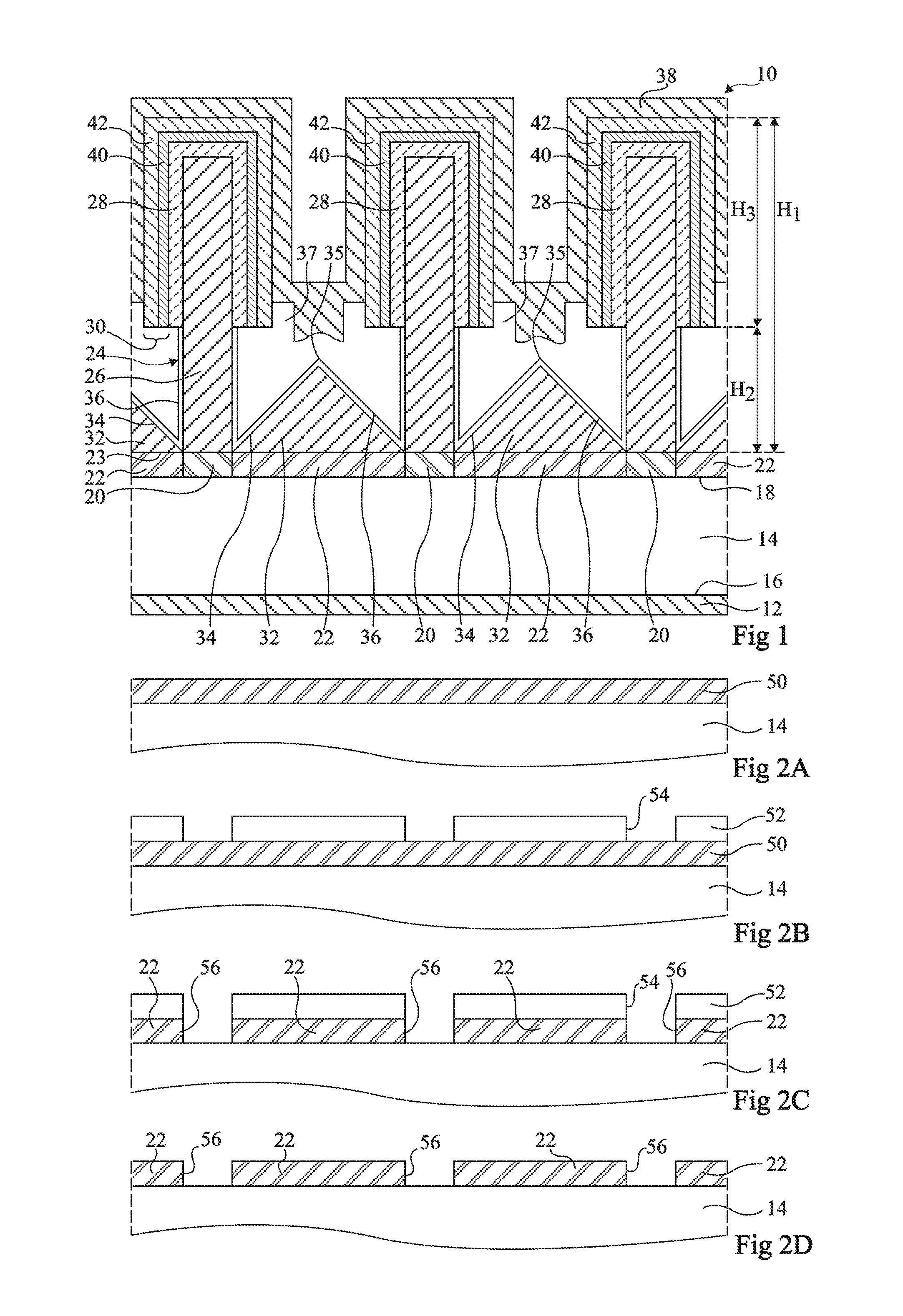
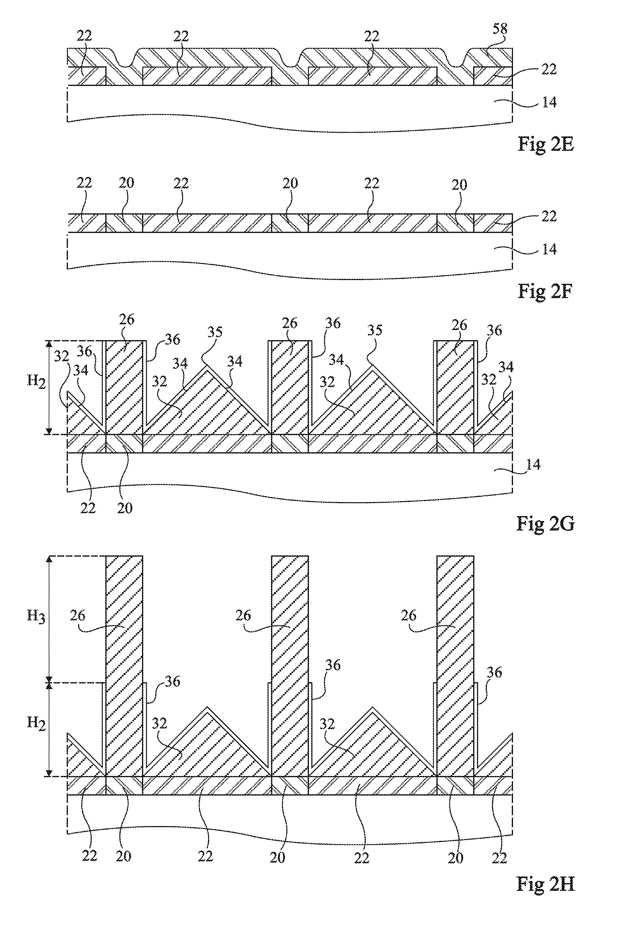
[0035]For clarity, the same elements have been designated with the same reference numerals in the different drawings and, further, as usual in the representation of electronic circuits, the various drawings are not to scale. Further, only those elements which are useful to the understanding of the present invention have been shown and will be described. In particular, the means for controlling the optoelectric devices described hereinafter are within the abilities of those skilled in the art and are not described.

[0036]In the following description, unless otherwise specified, terms “substantially”, “approximately”, and “on the order of” mean “to within 10%”. Further, “compound mainly formed of a material” or “compound based on a material” means that a compound comprises a proportion greater than or equal to 95% of said material, this proportion being preferentially greater than 99%.

[0037]The present invention relates to the manufacturing of microwires or nanowires. The term “microwi...


PUM


Abstract

An optoelectric device including microwires or nanowires on a support, each microwire or nanowire including at least one portion mainly containing a III-V compound in contact with the support, wherein the III-V compound is based on a first group-V element and on a second group-III element, wherein a surface of the support includes first areas of a first material promoting the growth of the III-V compound according to the polarity of the first element distributed in a second area of a second material promoting the growth of the compound according to the polarity of the second element, the microwires or nanowires being located on the first areas.

Description

CROSS-REFERENCE TO RELATED APPLICATIONS[0001]This is a continuation application of and claims priority to copending International Application Number PCT / FR2013 / 052128 having an international filing date of Sep. 17, 2013, which in turn claims priority to French Patent Application No. 1258729 filed Sep. 18, 2012, the entirety of each of the foregoing applications being hereby incorporated by reference herein for all purposes.BACKGROUND[0002]The present disclosure generally relates to semiconductor materials, to devices based on semiconductor materials, and to their manufacturing methods. The present disclosure more specifically relates to semiconductor microwires or nanowires and to devices comprising semiconductor microwires or nanowires.DISCUSSION OF THE RELATED ART[0003]Microwires or nanowires comprising a semiconductor material generally mainly containing a group-III element and a group-V element (for example, gallium nitride GaN), called III-V compounds hereafter, enable the manu...

Claims


Application Information

Patent Timeline
IPC IPC(8): H01L29/06H01L29/20H01L21/02
CPCH01L29/0657H01L21/02387H01L29/0673H01L29/068H01L21/02617H01L29/20H01L21/02603H01L21/0259H01L29/2003B82Y40/00H01L21/02381H01L21/02439H01L21/02458H01L21/0254H01L21/0262H01L21/02645H01L31/035227H01L31/184H01L31/1852H01L33/007H01L33/08H01L33/18H01L33/24Y02P70/50Y02E10/544
Inventor POUGEOISE, EMILIEDUSSAIGNE, AMELIE
Owner ALEDIA
Why Eureka
Try Eureka