Solid-state image sensor, method of manufacturing the same, and camera

a technology manufacturing method, which is applied in the field of solid-state image sensor, a method of manufacturing the same, and a camera, can solve the problems of color mixture and resolution degradation

Active Publication Date: 2014-03-20
CANON KK
View PDF4 Cites 3 Cited by
  • Summary
  • Abstract
  • Description
  • Claims
  • Application Information

AI Technical Summary

Benefits of technology

[0006]The present invention provides a technique advantageous in terms of isolation between pixels.

Problems solved by technology

Therefore, signals may mix between a plurality of photoelectric converters (pixels), thus leading to degradation in resolution and a mixture of colors.

Method used


Image

  • Solid-state image sensor, method of manufacturing the same, and camera
  • Solid-state image sensor, method of manufacturing the same, and camera
  • Solid-state image sensor, method of manufacturing the same, and camera

Examples


first embodiment

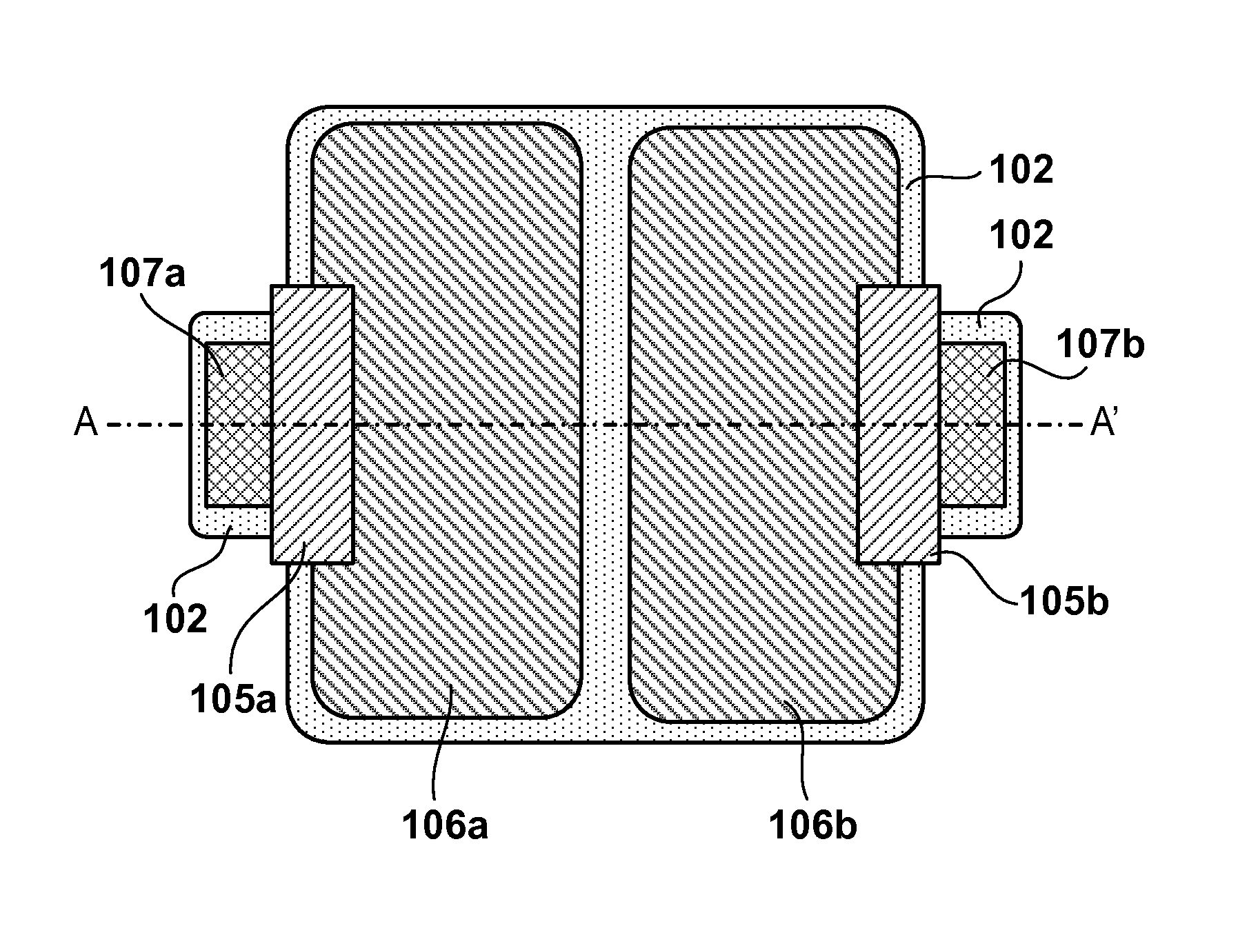
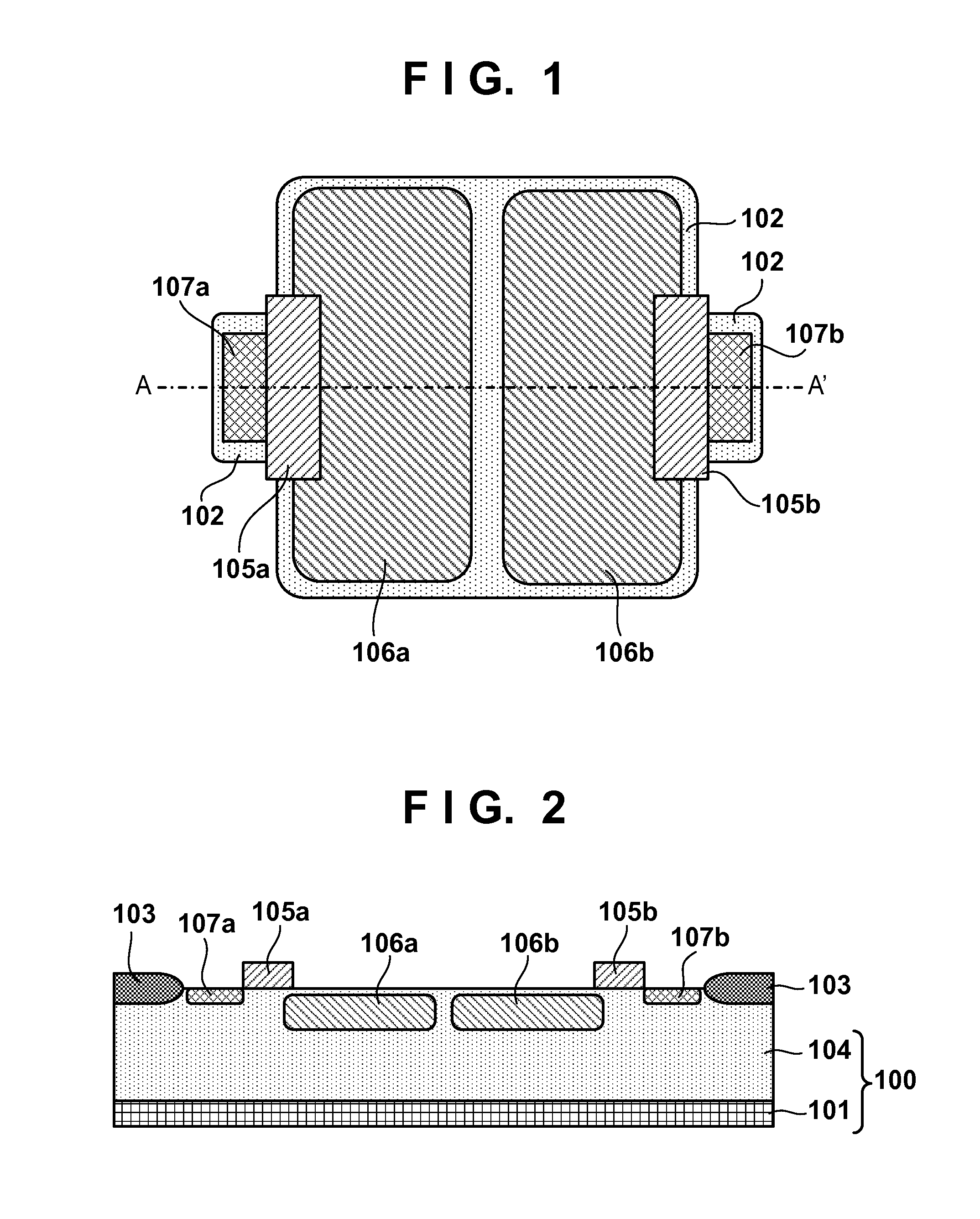
[0020]FIG. 1 is a plan view showing the partial arrangement of a pixel array of a solid-state image sensor according to the present invention, and FIG. 2 is a sectional view taken along a line A-A′ in FIG. 1. FIGS. 1 and 2 show the photoelectric converters and transfer gates of two pixels (first and second pixels). The first pixel includes a first photoelectric converter including a first charge accumulation region 106a, and a first transfer gate 105a which transfers charges accumulated in the first charge accumulation region 106a to a first charge-voltage converter 107a. The second pixel includes a second photoelectric converter including a second charge accumulation region 106b, and a second transfer gate 105b which transfers charges accumulated in the second charge accumulation region 106b to a second charge-voltage converter 107b. The first photoelectric converter can be formed by the first charge accumulation region 106a, and a well 104 present below it. The second photoelectri...

second embodiment

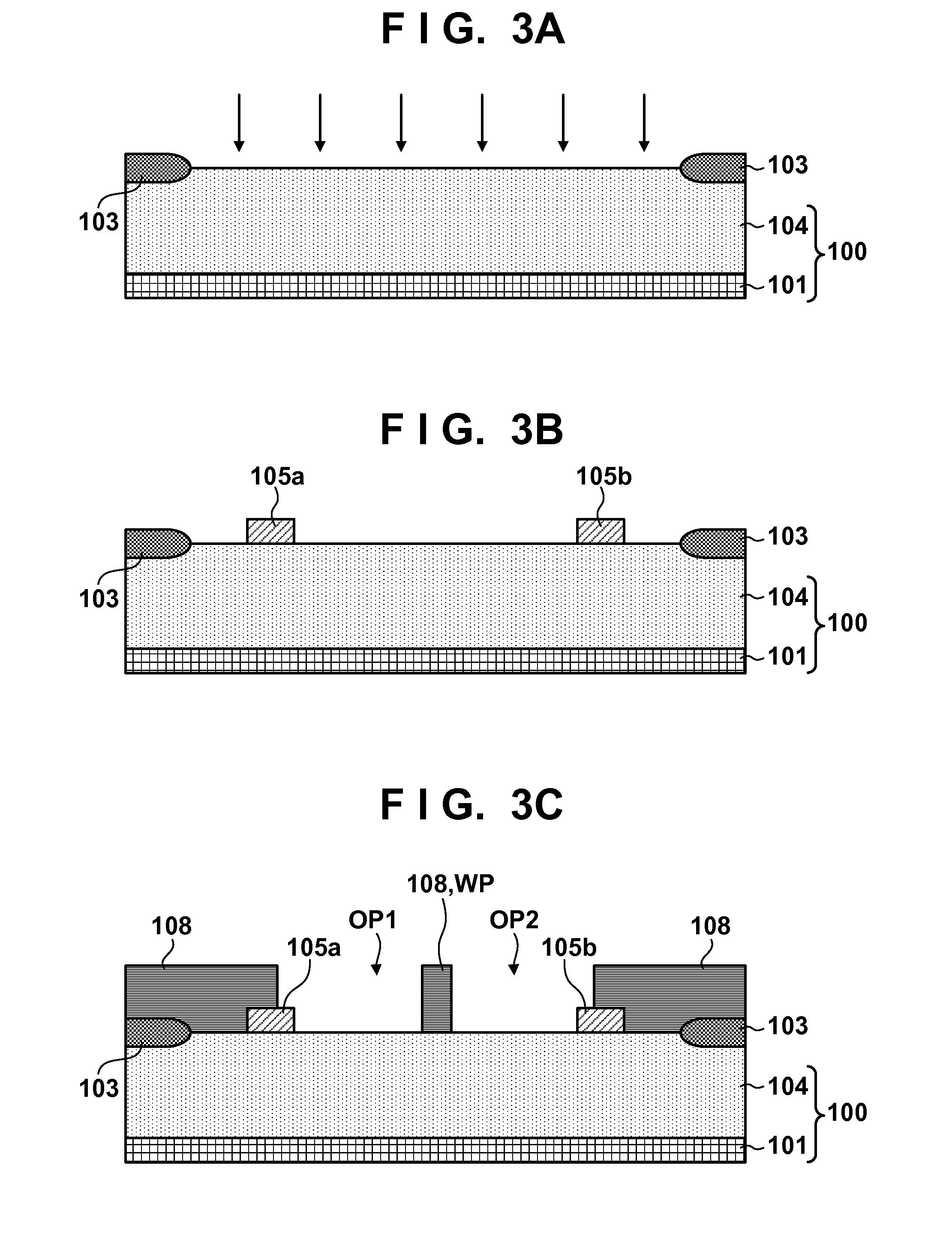
[0029]That is, in the second embodiment, the charge accumulation region forming step includes a first implantation step shown in FIG. 4A, a second implantation step shown in FIG. 4B, and a third implantation step shown in FIG. 5. Note that the procedure of execution of the first, second, and third implantation steps can be determined freely. In the third implantation step shown in FIG. 5, ions are implanted into a region deeper than that into which ions are implanted in the first and second implantation steps. In the third implantation step, a charge accumulation region 110a is formed below a first charge accumulation region 106a, while a charge accumulation region 110b is formed below a second charge accumulation region 106b. Note that the first charge accumulation region 106a and second charge accumulation region 106b can be referred to as upper charge accumulation regions hereinafter, while the charge accumulation regions 110a and 110b formed below them can be referred to as lowe...


PUM

PropertyMeasurementUnit
chargeaaaaaaaaaa
charge accumulationaaaaaaaaaa
angleaaaaaaaaaa

Abstract

A method of manufacturing a solid-state image sensor having a first charge accumulation region, a second charge accumulation region, includes implanting ions into a semiconductor substrate through first and second openings of a mask to form the first and second charge accumulation regions. The implanting ions includes a first implantation of implanting ions into a portion below a first transfer gate, and a second implantation of implanting ions into a portion below a second transfer gate in a direction different from a direction of the first implantation.

Description

BACKGROUND OF THE INVENTION[0001]1. Field of the Invention[0002]The present disclosure includes disclosure which relates to a solid-state image sensor, a method of manufacturing the same, and a camera.[0003]2. Description of the Related Art[0004]Patent literature 1 (Japanese Patent Laid-Open No. 6-209099) discloses the arrangement of a CCD solid-state image sensing element, and a method of manufacturing the same. A solid-state image sensor described in patent literature 1 has an N+-type impurity layer 5 isolated by a P++-type channel stopper layer 8 formed near the surface of a substrate, and an N−-type impurity layer 6 formed under transfer gate electrodes 10 to be adjacent to the N+-type impurity layer 5. In the manufacturing method described in patent literature 1, after the P++-type channel stopper layer 8 is formed near the surface of the substrate, phosphorus ions are implanted, into the region where a plurality of photoelectric converters are to be formed between a pair of tr...

Claims


Application Information

Patent Timeline
Patent Type & Authority Applications(United States)
IPC IPC(8): H01L31/0232H01L31/18
CPCH01L31/18H01L31/02327H01L27/1461H01L27/14689
Inventor TSUCHIYA, MASAYUKI
Owner CANON KK
Why Eureka
Try Eureka