

Supply circuit in a communication system of a protective headgear, protective headgear with such a supply circuit and method for operating such a supply circuit
a communication system and supply circuit technology, applied in the direction of emergency protective arrangements for limiting excess voltage/current, electric variable regulation, transmission, etc., can solve the problems of non-rechargeable batteries, large work and testing effort, and the need for a power source that can be carried along, so as to avoid explosion hazards, reduce the probability of malfunction based on defects or tolerances, and avoid explosion hazards
- Summary
- Abstract
- Description
- Claims
- Application Information
AI Technical Summary
Benefits of technology
Problems solved by technology
Method used
Image

Examples
Embodiment Construction
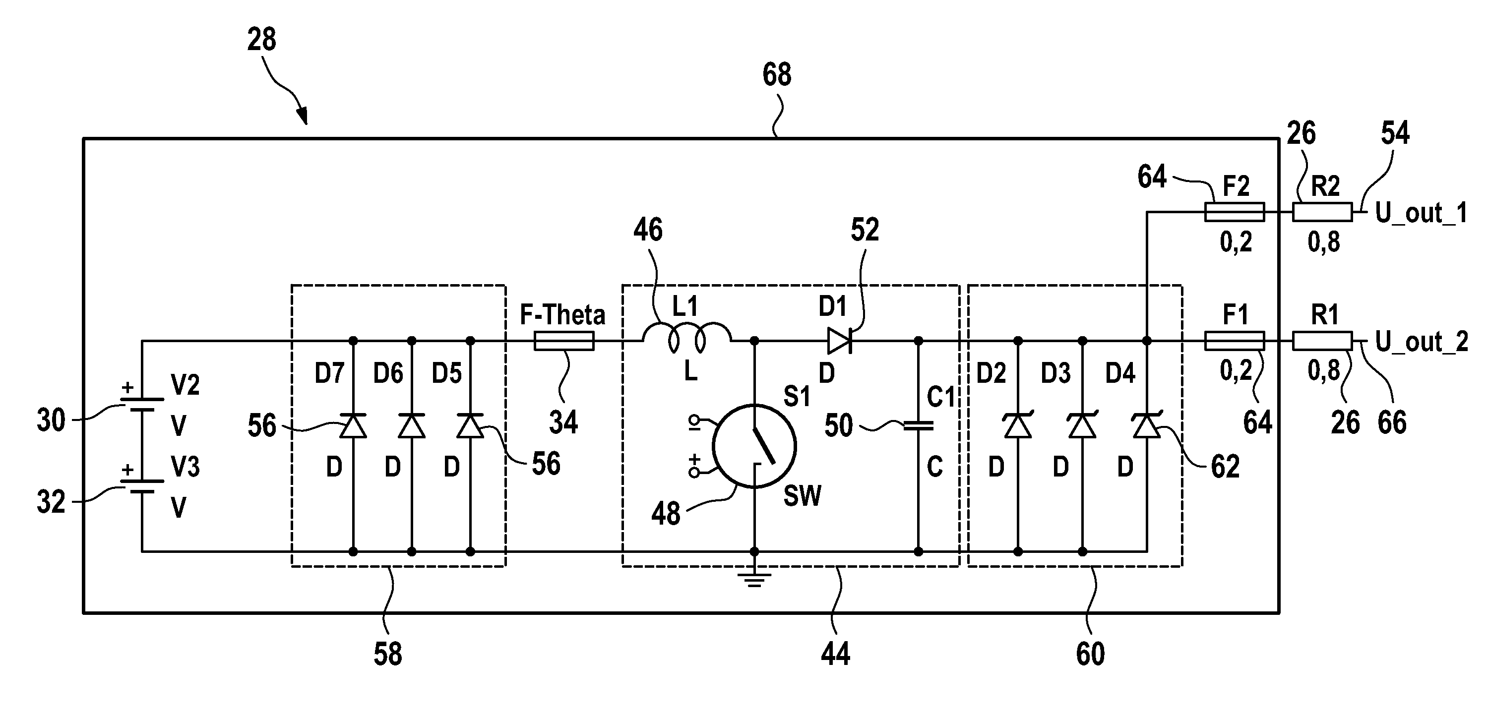
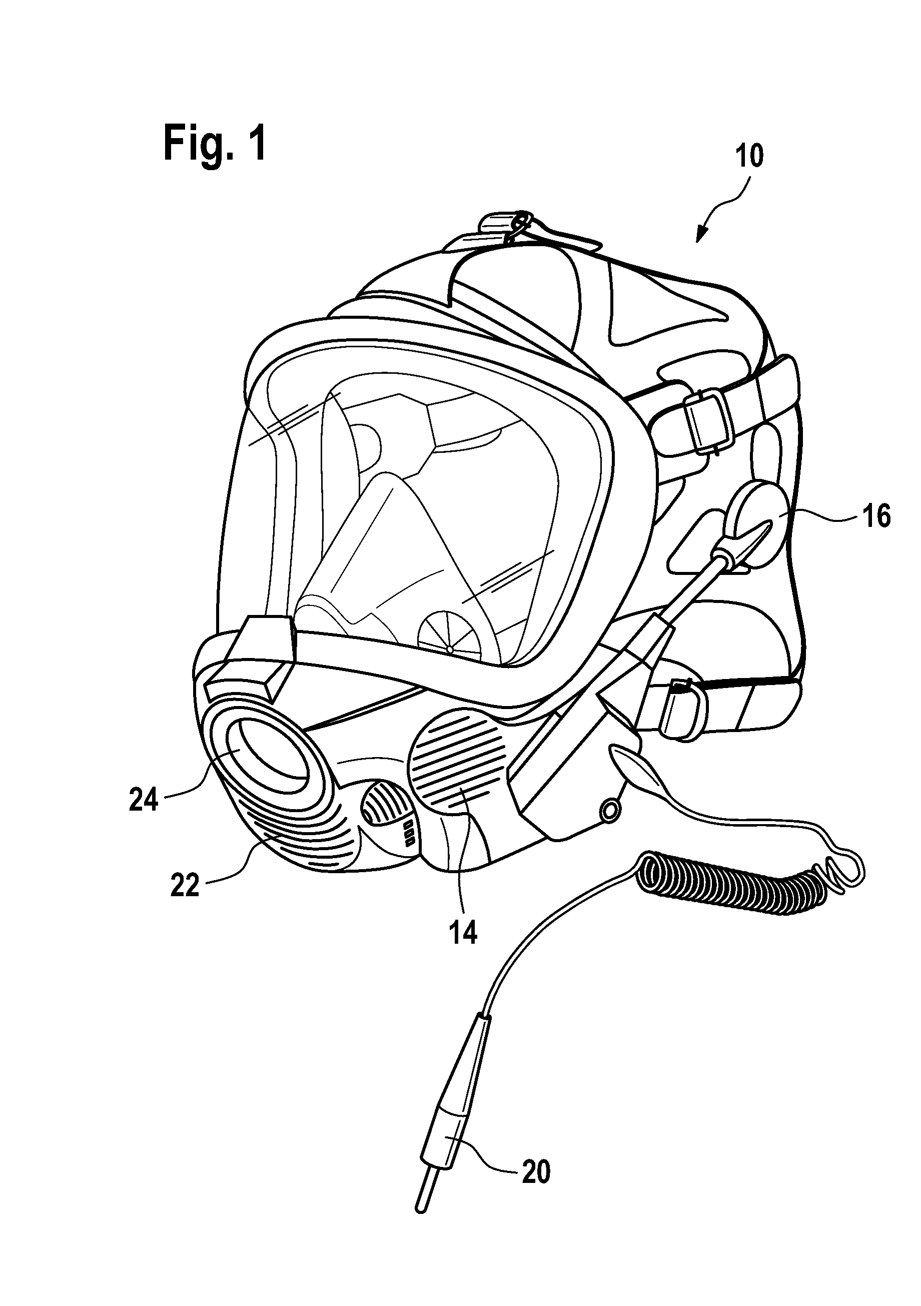
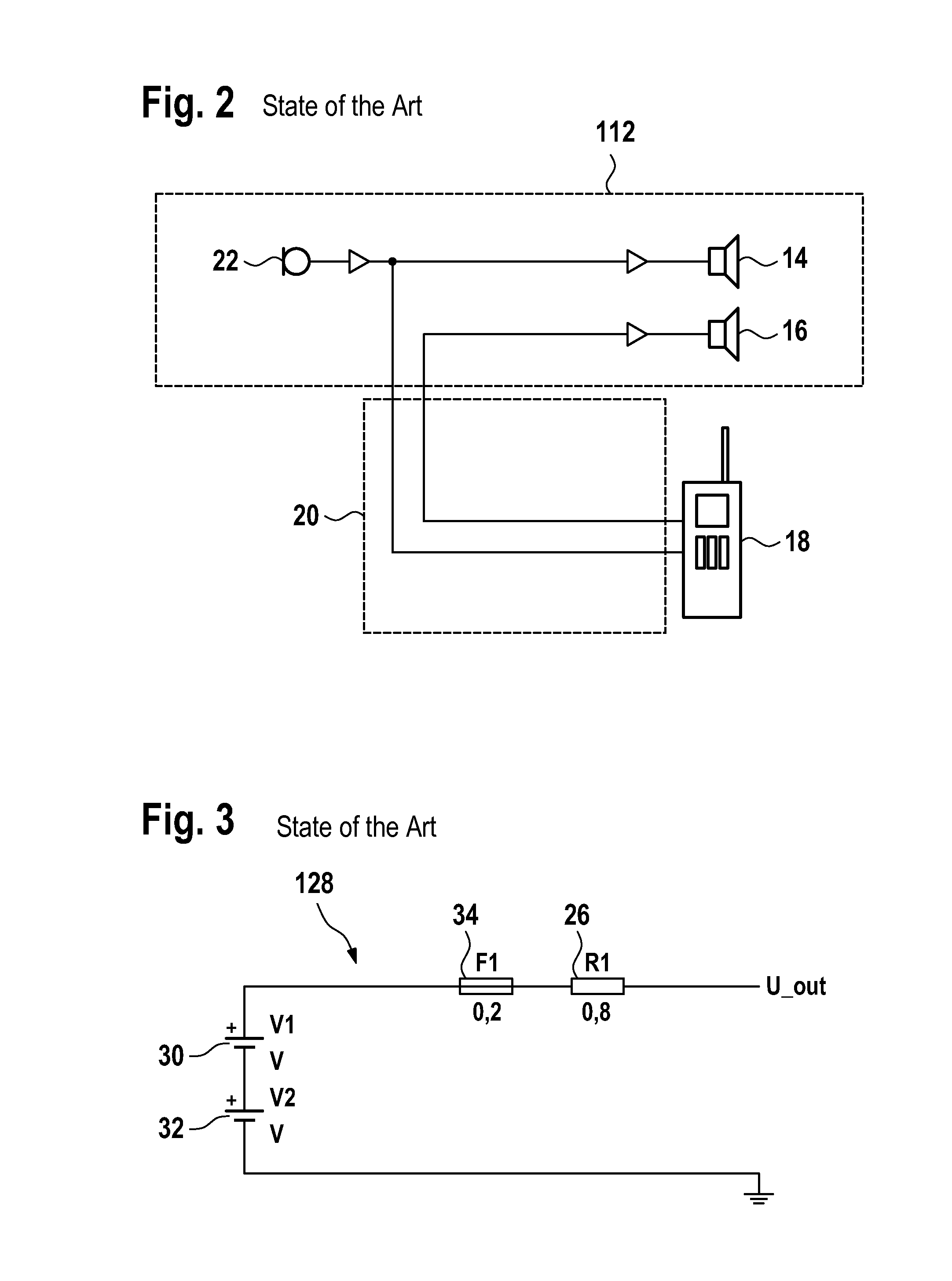
[0030]Referring to the drawings in particular, FIG. 1 shows a so-called full face mask as an example of protective headgear 10, as it is in the foreground here. A mask communication system designated here and below by 112 (FIG. 2) for short is integrated here in the protective headgear 10, namely, in the outer contour of the protective headgear 10. Loudspeaker 14 is located on one side or on both sides of the protective headgear 10 as components of the communication system 112. In addition, an earphone 16 (it is also possible to provide two earphones if necessary), which can reproduce the signal of a tactical radio equipment 17 (FIG. 2) at the ear of the user of the protective headgear 10, can be recognized. The connection with the radio equipment 18, which the user of the protective headgear 10 brings along with him in a suitable manner, for example, on a belt, is brought about by means of a cable 20, and a microphone 22 for receiving the speech signal is located in the interior of...
PUM
 Abstract
Description
Claims
Application Information