Structures and devices including a tensile-stressed silicon arsenic layer and methods of forming same

Active Publication Date: 2014-03-27
ASM IP HLDG BV
View PDF12 Cites 364 Cited by
  • Summary
  • Abstract
  • Description
  • Claims
  • Application Information

AI Technical Summary

Benefits of technology

[0006]Various embodiments of the present disclosure relate to structures and devices including a tensile-stressed silicon region or layer and to methods of forming the structures and devices. While the ways in which various embodiments of the disclosure address the drawbacks of the prior art structures, devices, and methods are discussed in more detail below, in general, the present disclosure provides methods of forming a tensile-stressed silicon layer us

Problems solved by technology

Although doping silicon with carbon can create a tensile stress within a silicon lattice, adding carbon to the si

Method used


Image

  • Structures and devices including a tensile-stressed silicon arsenic layer and methods of forming same
  • Structures and devices including a tensile-stressed silicon arsenic layer and methods of forming same
  • Structures and devices including a tensile-stressed silicon arsenic layer and methods of forming same

Examples


Embodiment Construction

[0026]The description of exemplary embodiments of methods, structures, and devices provided below is merely exemplary and is intended for purposes of illustration only; the following description is not intended to limit the scope of the disclosure or the claims. Moreover, recitation of multiple embodiments having stated features is not intended to exclude other embodiments having additional features or other embodiments incorporating different combinations of the stated features.

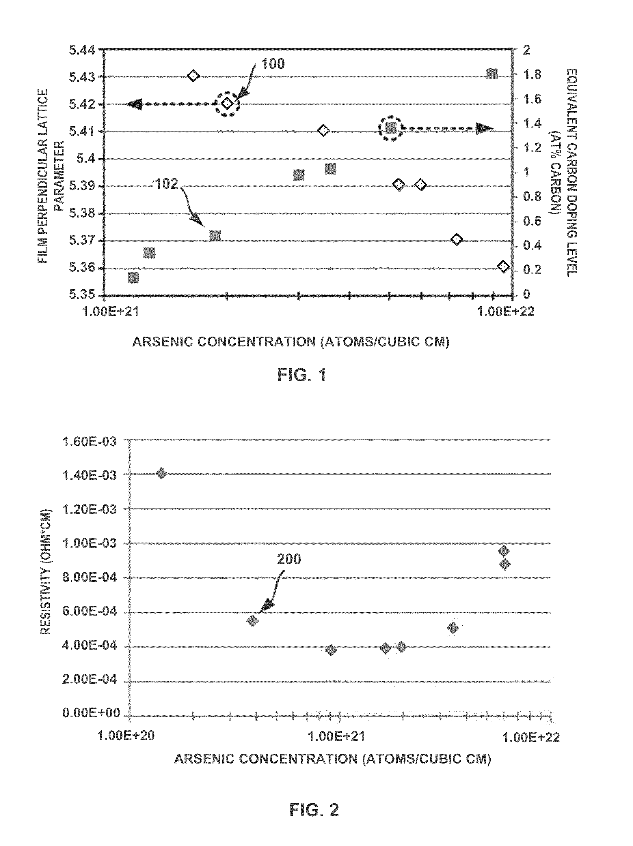
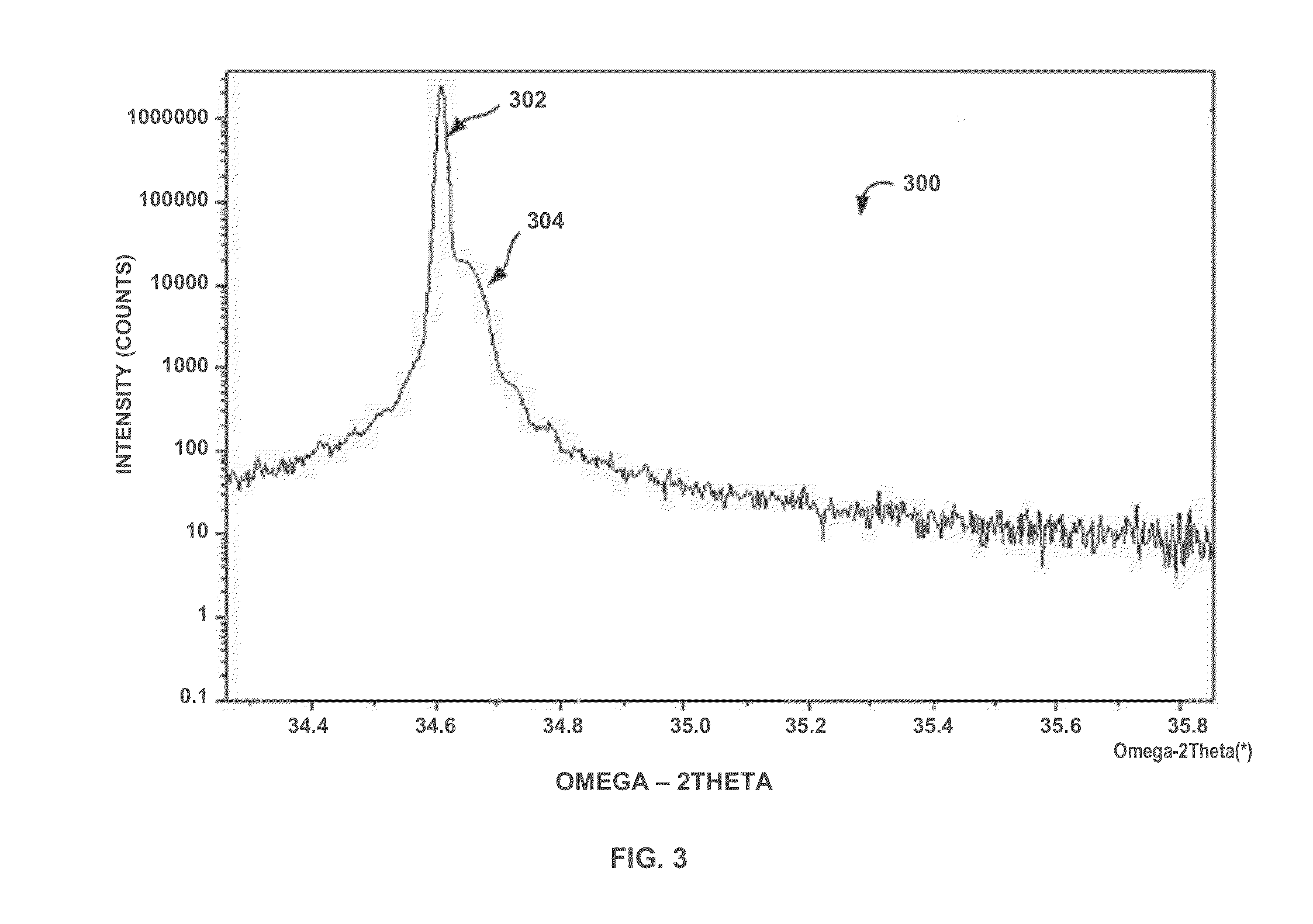
[0027]The present disclosure generally relates to structures and devices that include a tensile-stressed silicon layer and to methods of forming the structures and devices. As used herein, a tensile stress refers to a stress imparted to a first material having a smaller lattice spacing relative to a lattice spacing of a second material to which the first material is bound / adhered. Because the atoms of the first material are held at a greater distance from one another by spacing of atoms in the second materia...


PUM


Abstract

Structures including a tensile-stressed silicon arsenic layer, devices including the structures, and methods of forming the devices and structures are disclosed. Exemplary tensile-stressed silicon arsenic layer have an arsenic doping level of greater than 5 E+20 arsenic atoms per cubic centimeter. The structures can be used to form metal oxide semiconductor devices.

Description

CROSS REFERENCE TO RELATED APPLICATION[0001]This application claims the benefit and priority of Provisional Application No. 61 / 705,932, filed on Sep. 26, 2012, entitled TENSILE STRESSED SILICON-ARSENIC ALLOYS, the contents of which are hereby incorporated by reference to the extent the contents do not conflict with the present disclosure.FIELD OF INVENTION[0002]The present disclosure generally relates to semiconductor structures and devices and to methods of forming the structures and devices. More particularly, the disclosure relates to structures and devices that include a silicon arsenic layer and to methods of forming the structures and devices.BACKGROUND OF THE DISCLOSURE[0003]Semiconductor devices may include a tensile-stressed layer for a variety of reasons. For example, metal oxide semiconductor (MOS) devices may include a tensile-stressed layer, which forms part of a channel region of the devices. The tensile-stressed layer may exhibit higher carrier mobility—compared to a ...

Claims


Application Information

Patent Timeline
IPC IPC(8): H01L29/267H01L21/02
CPCH01L21/02532H01L29/267H01L21/02521H01L21/02576H01L21/0262H01L21/67207H01L29/1054H01L21/18H01L21/20H01L21/265H01L29/7851
Inventor WEEKS, KEITH DORAN
Owner ASM IP HLDG BV
Why Eureka
Try Eureka