Electronic component mounting method, electronic component placement machine, and electronic component mounting system

a technology for electronic components and mounting methods, applied in the direction of manufacturing tools, sustainable manufacturing/processing, final product manufacturing, etc., can solve the problem that the strength of the solder joints may not be sufficient, and achieve the effect of preventing the junction of the solder joints, better understanding and better understanding

Active Publication Date: 2014-04-10
PANASONIC INTELLECTUAL PROPERTY MANAGEMENT CO LTD
View PDF11 Cites 7 Cited by
  • Summary
  • Abstract
  • Description
  • Claims
  • Application Information

AI Technical Summary

Benefits of technology

[0121]According to the electronic component mounting method, the electronic component placement machine, and the electronic component mounting system of the present invention, even when the thermosetting resin dispensed as the reinforcing resin coats the electrodes provided on the substrate, the electrodes are sufficiently wetted with the molten bumps during reflowing. Therefore, poor junction at the solder joints can be prevented.
[0122]While the novel features of the invention are set forth particularly in the appended claims, the invention, both as to organization and content, will be better understood and appreciated, along with other objects and features thereof, from the following detailed description taken in conjunction with the drawings.

Problems solved by technology

When thermal stress generated by thermal cycling, or external force, is applied to a mounting structure comprising a substrate and electronic components obtained through the aforementioned mounting process, and if the electronic components are joined to the substrate via the bumps, the solder joints may lack sufficient strength.

Method used


Image

  • Electronic component mounting method, electronic component placement machine, and electronic component mounting system
  • Electronic component mounting method, electronic component placement machine, and electronic component mounting system
  • Electronic component mounting method, electronic component placement machine, and electronic component mounting system

Examples


Embodiment Construction

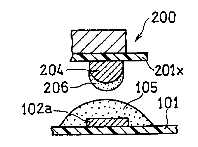
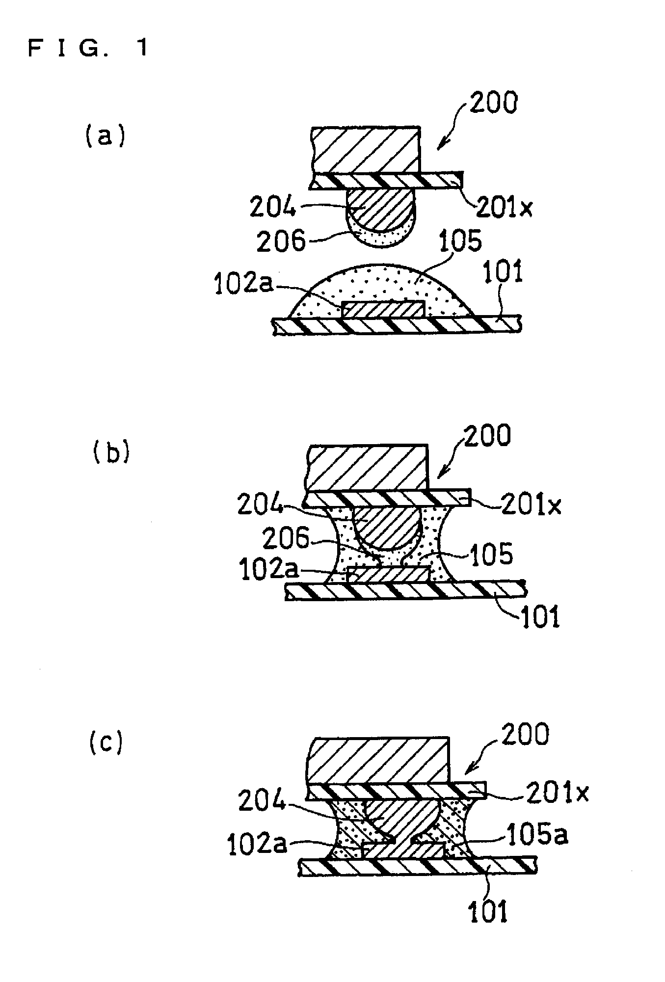
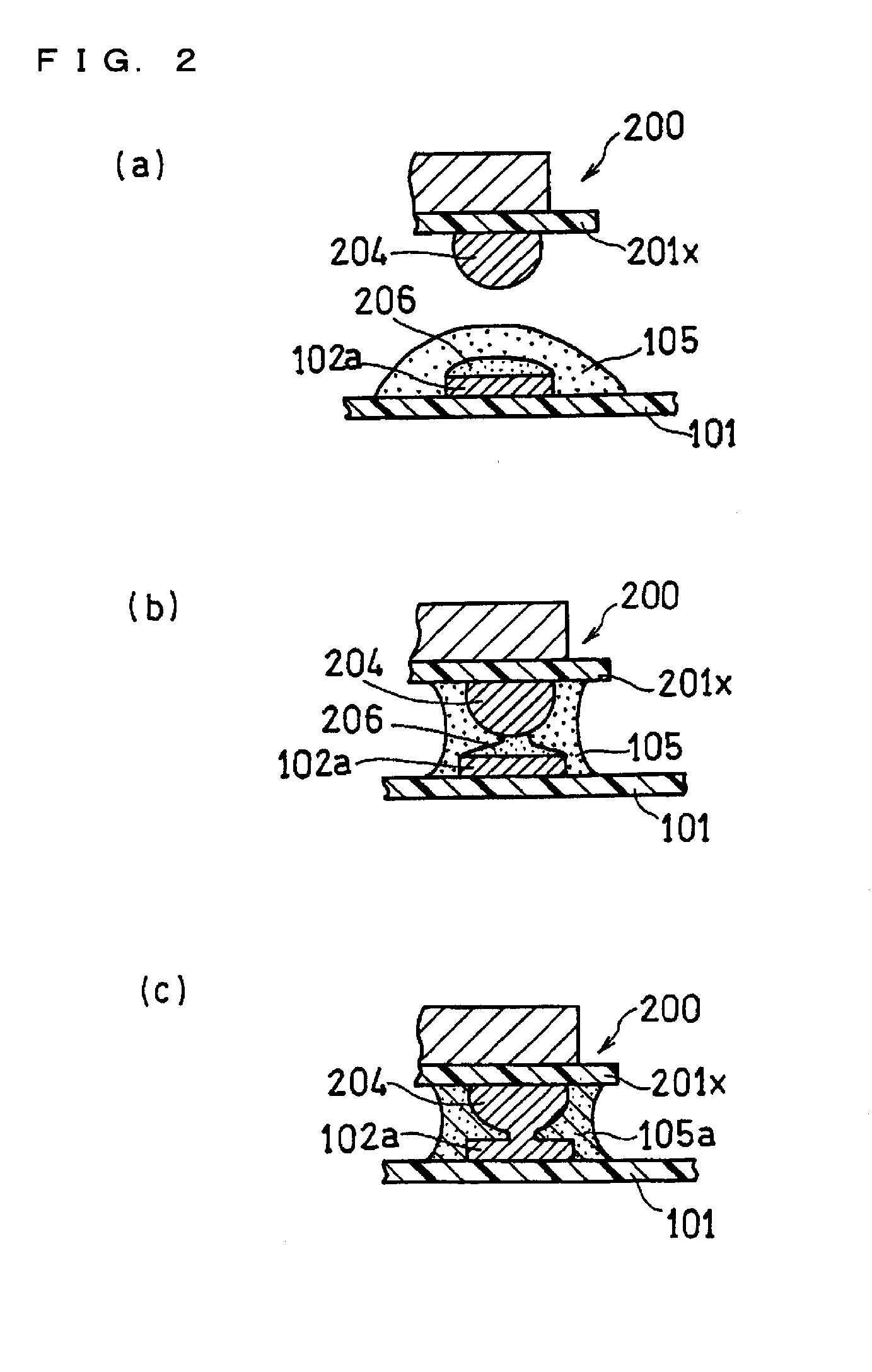
[0145]First, an electronic component mounting method according to one embodiment of the present invention is described.

[0146]Here, a description is given with reference to a typical mounting structure which includes: a ball grid array (BGA) electronic component (first electronic component) to be connected to electrodes (lands) of a substrate via a plurality of bumps; and an electronic component (second electronic component) to be connected to the electrodes on the substrate via a paste containing metal particles such as cream solder.

[0147]First, a substrate, a first electronic component, and a second electronic component are prepared.

[0148]FIG. 3A is a longitudinal sectional view of an example of a first electronic component 200, and FIG. 3B is a bottom view thereof.

[0149]The first electronic component 200 is a package including a thin substrate (inner substrate) 201, a semiconductor element 202 mounted on the upper surface thereof, and a resin sealant 203 encapsulating the semicond...


PUM

PropertyMeasurementUnit
areaaaaaaaaaaa
thermal stressaaaaaaaaaa
strengthaaaaaaaaaa

Abstract

An electronic component mounting method including the steps of: providing a first electronic component having a principal surface provided with a plurality of bumps; providing a substrate having a placement area provided with a plurality of first electrodes corresponding to the plurality of bumps; applying flux to the plurality of bumps; applying flux to at least one of the first electrodes adjacent to at least one reinforcement position set on a peripheral portion of the placement area; dispensing a thermosetting resin onto the reinforcement position, and at least partially coating the first electrode adjacent to the reinforcement position, with the thermosetting resin; placing the first electronic component on the substrate such that the bumps land on the corresponding first electrodes, and thus bringing the thermosetting resin into contact with a peripheral edge portion of the first electronic component; and heating the substrate with the first electronic component placed thereon.

Description

TECHNICAL FIELD[0001]The present invention relates to a method and a machine for placing or mounting on a substrate, an electronic component having a plurality of bumps.BACKGROUND ART[0002]Various electronic components are incorporated in electronic devices. These electronic components are joined at predetermined positions on a substrate having a plurality of electrodes and lead frames, and are incorporated as such as a mounting structure in the devices. With the advancement of miniaturization of electronic devices in recent years, the electronic components incorporated in the devices are being more and more miniaturized, thus causing increased use of small-sized electronic components such as flip chips and chip size packages (CSPs) to be placed on a substrate.[0003]Electronic components such as flip chips and CSPs have a principal surface on which a plurality of terminals are regularly arranged in an array, and each terminal has a solder bump formed thereon. In mounting such an ele...

Claims


Application Information

Patent Timeline
Patent Type & Authority Applications(United States)
IPC IPC(8): H05K3/30
CPCH05K3/305H01L24/13H01L24/16H01L24/29H01L24/32H01L24/73H01L24/75H01L24/81H01L24/83H01L24/92H01L2224/11822H01L2224/131H01L2224/16225H01L2224/16265H01L2224/29012H01L2224/29078H01L2224/2919H01L2224/30155H01L2224/32225H01L2224/73103H01L2224/73104H01L2224/73203H01L2224/73204H01L2224/7501H01L2224/7515H01L2224/75611H01L2224/75821H01L2224/81011H01L2224/8102H01L2224/81024H01L2224/81143H01L2224/81193H01L2224/81815H01L2224/81903H01L2224/81986H01L2224/83104H01L2224/83192H01L2224/83194H01L2224/8385H01L2224/83862H01L2224/9211H01L2924/19105H01L2924/351H05K3/3436H05K13/0465H05K2201/10977Y10T29/4913Y10T29/49144Y10T29/49146Y10T29/49149Y10T29/49179Y10T29/53174Y02P70/50H01L2924/00H01L2924/00014H01L2924/00012H01L2924/014H01L2224/81H01L2224/83H01L2224/9205H05K3/34H05K3/3405H05K3/3468H05K3/3489H05K3/3494H05K3/3485
Inventor SAEKI, TSUBASAWADA, YOSHIYUKIMOTOMURA, KOJISAKAI, TADAHIKO
Owner PANASONIC INTELLECTUAL PROPERTY MANAGEMENT CO LTD
Why Eureka
Try Eureka