Circuit and method for biasing a plate-shaped sensor element of semiconductor material

a sensor element and circuit technology, applied in the direction of solid-state devices, magnetic field measurement using galvano-magnetic devices, instruments, etc., can solve the problems of not being completely true, affecting the sensitivity and linearity of the magnetic sensor, and may not be suitable for all contemporary cmos technologies

Active Publication Date: 2014-04-17
MELEXIS TECH NV
View PDF4 Cites 50 Cited by
  • Summary
  • Abstract
  • Description
  • Claims
  • Application Information

AI Technical Summary

Benefits of technology

[0012]It is an object of embodiments of the present invention to provide a good method for biasing a plate-shaped sensor element made of doped semiconductor material.
[0013]In particular, it is an object of embodiments of the present invention to provide a method for biasing a plate-shaped sensor element made of doped semiconductor material which is better suitable for contemporary technologies, in particular CMOS technologies, and which has a similar performance as the prior art circuits, preferably even better.

Problems solved by technology

Unfortunately, when using current biasing, the effectively applied voltages (between nodes A and C) depend strongly on temperature, but also piezoresistive stress-effects and even the Hall effect itself affects the voltages (i.e. the voltages also vary in the X-direction of FIG. 2).
Because these effects modulate the thickness of the plate, they affect the sensitivity and the linearity of the magnetic sensor.
In practice, however, this is not entirely true.
However, this circuit may not be suitable for all contemporary CMOS technologies, as the potential of all the shielding regions cannot always be chosen freely.
Furthermore, the practical approach to biasing shown in FIG. 3 is not fully specified.
In practice, it is not always possible to change the potential of the shield, especially when the substrate is part of the surrounding shield.
In the circuit of FIG. 5(a), a large common mode voltage exists, which is disadvantageous for accurate amplification.

Method used


Image

  • Circuit and method for biasing a plate-shaped sensor element of semiconductor material
  • Circuit and method for biasing a plate-shaped sensor element of semiconductor material
  • Circuit and method for biasing a plate-shaped sensor element of semiconductor material

Examples


Embodiment Construction

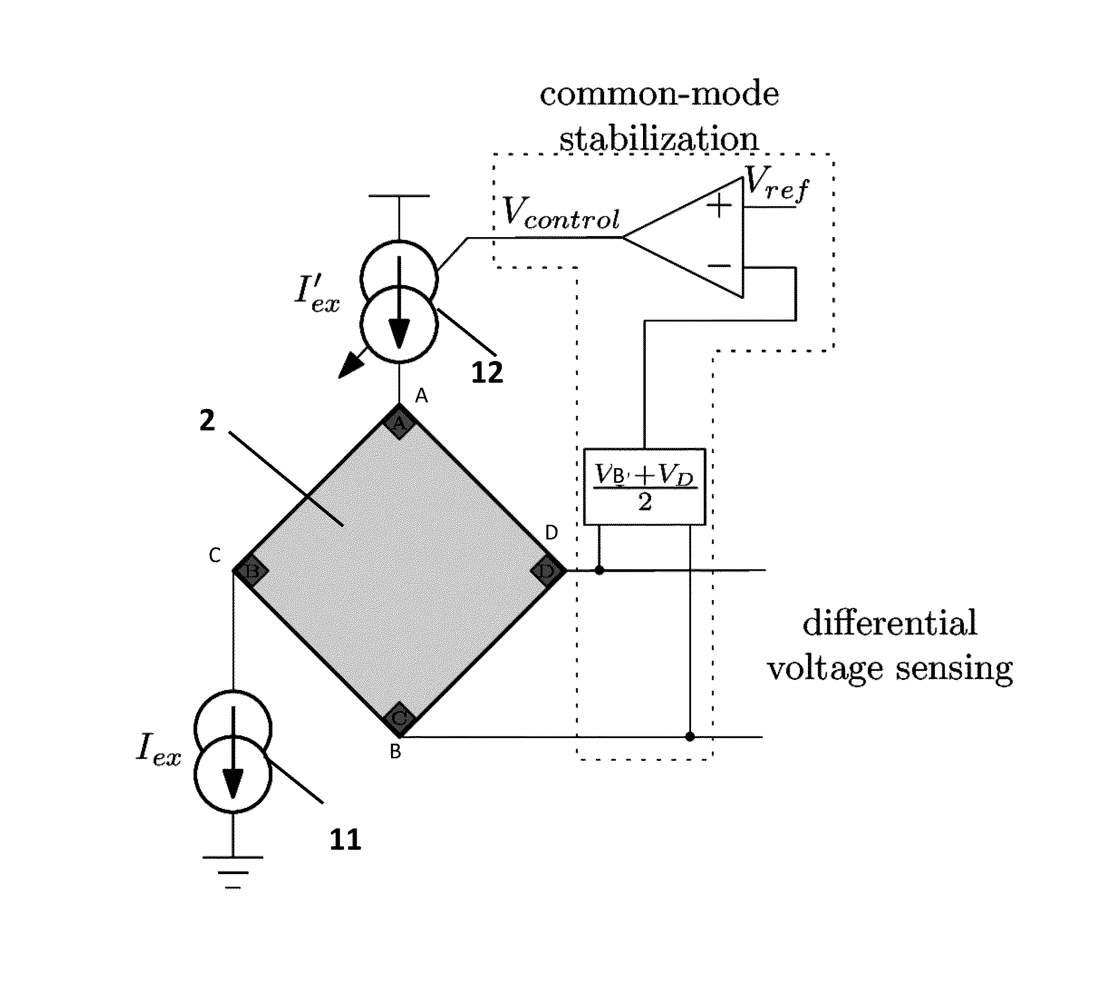
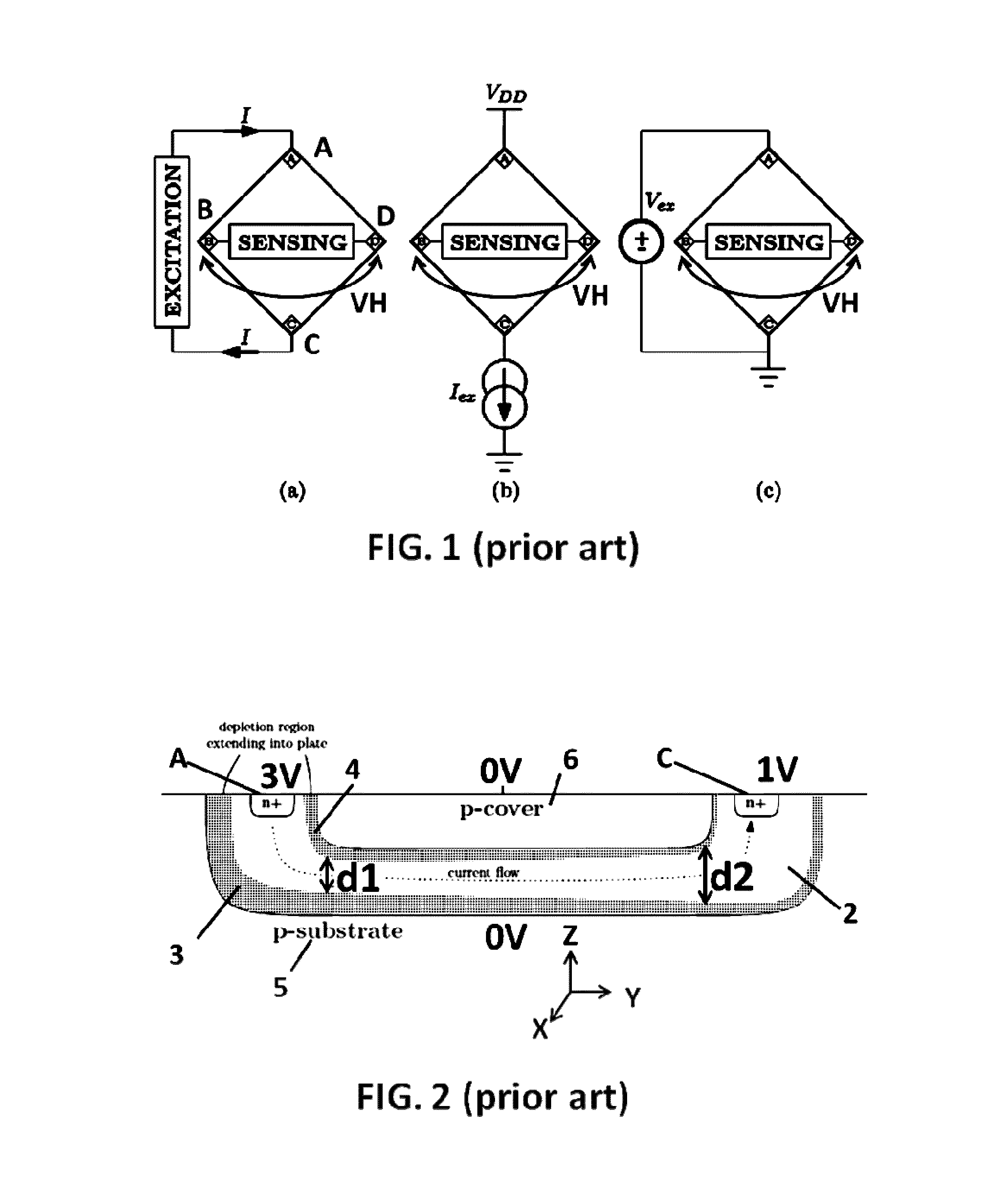
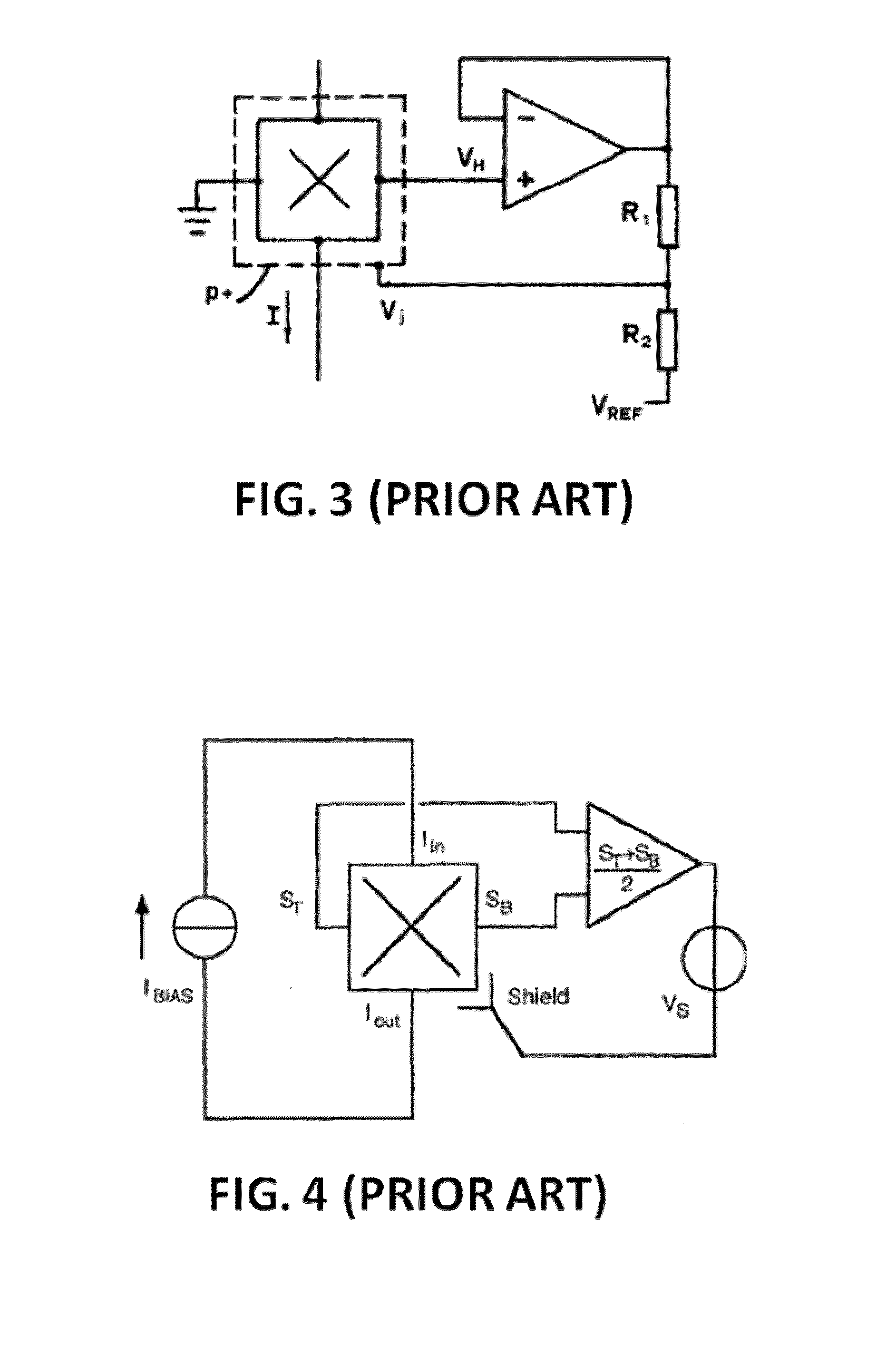
[0096]The present invention will be described with respect to particular embodiments and with reference to certain drawings but the invention is not limited thereto but only by the claims. The drawings described are only schematic and are non-limiting. In the drawings, the size of some of the elements may be exaggerated and not drawn on scale for illustrative purposes. The dimensions and the relative dimensions do not correspond to actual reductions to practice of the invention.

[0097]The terms first, second and the like in the description and in the claims, are used for distinguishing between similar elements and not necessarily for describing a sequence, either temporally, spatially, in ranking or in any other manner. It is to be understood that the terms so used are interchangeable under appropriate circumstances and that the embodiments of the invention described herein are capable of operation in other sequences than described or illustrated herein.

[0098]Moreover, the terms top,...


PUM


Abstract

Circuit and method for biasing a plate-shaped sensor element (2) made of doped semiconductor material and having a first resp. second excitation contact (C, A) connected to a first resp. second excitation node (Cn, An), and a first resp. second sense contact (B, D) connected to a first resp. second sense node (Bn, Dn). The plate-shaped sensor element is electrically isolated from a substrate or well (5) by means of a first PN-junction. The method comprises: a) applying to the first excitation node (Cn) a predefined first current (Iex) generated by a first current source (11); b) applying to the second excitation node (An) a second current (I′ex) generated by a controllable second source (12); c) controlling the second source (12) by means of a negative feedback loop based on a comparison between a value representative for a common mode voltage (Vcm) of the voltages (VB, VD) of the sense nodes (Bn, Dn) and a predefined reference voltage (Vref), such that the common mode voltage (Vcm) is substantially equal to the reference voltage (Vref).

Description

FIELD OF THE INVENTION[0001]The present invention relates to the field of biasing plate-shaped sensor elements of semiconductor material, such as for instance Hall elements (also called “Hall plates”), in particular for example integrated junction-isolated Hall elements, or sensor elements having a Van der Pauw structures, such as for instance a Van der Pauw stress sensor.BACKGROUND OF THE INVENTION[0002]Plate-shaped sensor elements of semiconductor material are applied in Hall elements and in other sensor elements having a Van der Pauw structure, such as the stress sensor known from Mian, A.; Suhling, J. C.; Jaeger, R. C., “The van der Pauw stress sensor,” Sensors Journal, IEEE, vol. 6, no. 2, pp. 340, 356, April 2006. Both the Hall elements and the sensor elements having a Van der Pauw structure are constructionally similar to one another, but use different measurements to derive information on the physical quantity to be measured (e.g. magnetic field versus stress).[0003]Hall sen...

Claims


Application Information

Patent Timeline
Patent Type & Authority Applications(United States)
IPC IPC(8): G01R33/07G01R33/09
CPCG01R33/09G01R33/07G01R33/0023G01R33/0041G01R33/007H10B61/00H10N59/00H10N52/80
Inventor RAMAN, JOHANROMBOUTS, PIETER
Owner MELEXIS TECH NV
Why Eureka
Try Eureka