Semiconductor package and method of fabricating the same

a technology of semiconductor devices and packages, applied in the direction of semiconductor devices, semiconductor/solid-state device details, electrical apparatus, etc., to achieve the effect of preventing package warpage and significantly improving the alignment accuracy of subsequent processes

Inactive Publication Date: 2014-05-01
SILICONWARE PRECISION IND CO LTD
View PDF6 Cites 7 Cited by
  • Summary
  • Abstract
  • Description
  • Claims
  • Application Information

AI Technical Summary

Benefits of technology

[0013]Compared with the prior art, the method of fabricating a semiconductor package according to the present invention performs a thermal compression process after the semiconductor chip is wrapped by the positioning member layer. Therefore, the die shift problem of the semiconductor chip is limited by the positioning member layer, and the alignment accuracy of subsequent processes is improved significantly.
[0014]In the embodiment, before the carrier and the soft material layer are removed, a supporting layer is further formed on the top surface of the encapsulant, such that the encapsulant is encapsulated between the supporting layer and the positioning member layer to prevent the package from warpage.

Problems solved by technology

Therefore, it is an urgent issue in the art to provide a semiconductor package and a method of fabricating the same, in which buried conductive vias are electrically connected to electrode pads perfectly.

Method used


Image

  • Semiconductor package and method of fabricating the same
  • Semiconductor package and method of fabricating the same
  • Semiconductor package and method of fabricating the same

Examples


Embodiment Construction

[0022]The following illustrative embodiments are provided to illustrate the disclosure of the present invention, these and other advantages and effects can be apparently understood by those in the art after reading the disclosure of this specification. The present invention can also be performed or applied by other different embodiments. The details of the specification may be on the basis of different points and applications, and numerous modifications and variations can be devised without departing from the spirit of the present invention.

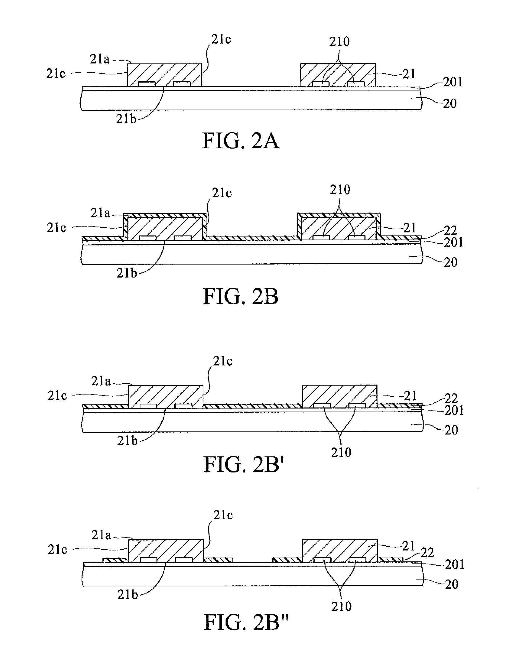
[0023]Referring to FIGS. 2A-2F′, cross-sectional diagrams illustrating a method of fabricating a semiconductor package in accordance with one embodiment of the present invention are provided.

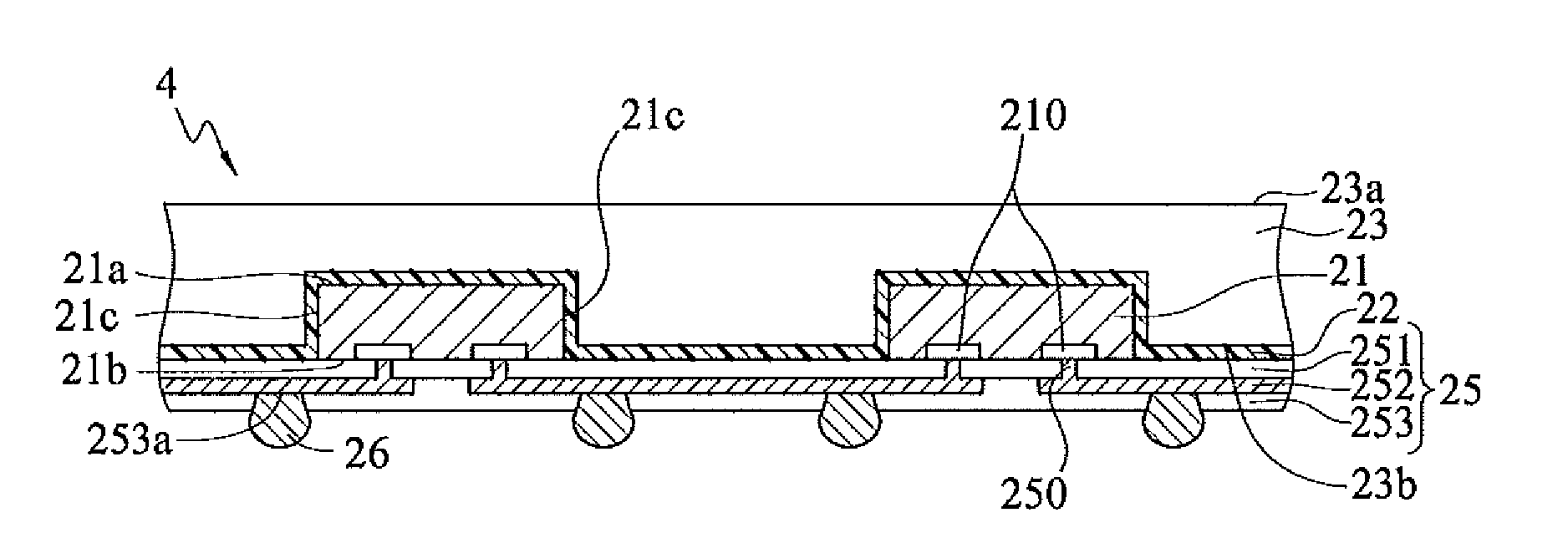
[0024]Referring to FIG. 2A, a carrier 20 has a surface formed with at least a semiconductor chip 21. The semiconductor chip 21 has an active surface 21b, and an inactive surface 21a opposite to the active surface 21a. The active surface 21b of the semiconduct...


PUM


Abstract

Disclosed is a semiconductor package including an encapsulant having a top surface and a bottom surface opposite to the top surface; a semiconductor chip embedded in the encapsulant having an active surface, an inactive surface opposite to the active surface, and lateral surfaces interconnecting the active surface and the inactive surface, wherein the active surface protrudes from the bottom surface of the encapsulant and the semiconductor chip further has a plurality of electrode pads disposed on the active surface; a positioning member layer formed on a portion of the bottom surface of the encapsulant, covering the lateral surfaces of the semiconductor chip that protrude therefrom, and exposing the active surface; and a build-up trace structure disposed on the active surface of the semiconductor chip and the positioning member layer formed on the bottom surface of the encapsulant. The present invention also provides a method of fabricating a semiconductor package.

Description

BACKGROUND OF THE INVENTION[0001]1. Field of the Invention[0002]This invention relates to semiconductor packages and methods of fabricating the same, and more particularly, to a semiconductor package that can resolve a die shift problem and a method of fabricating the semiconductor package.[0003]2. Description of Related Art[0004]With the rapid development of semiconductor technology, there are various types of semiconductor package products to meet application requirements. In order to fabricate compact-sized and low-profiled semiconductor packages, a WL-CSP (wafer level chip scale package) has been developed to provide a surface area large enough to carry a sufficient number of I / O (input / output) terminals and to utilize RDL (redistribution layer) technology to form an RDL on a semiconductor chip such that a plurality of bonding pads on the semiconductor chip are then redistributed via the RDL to the designed optimal positions as I / O (input / output) terminals.[0005]However, in a me...

Claims


Application Information

Patent Timeline
Patent Type & Authority Applications(United States)
IPC IPC(8): H01L23/498H01L21/56
CPCH01L23/49811H01L21/56H01L23/3128H01L23/5389H01L24/19H01L24/96H01L2224/04105H01L2224/12105H01L2224/24137H01L23/3107H01L21/561H01L21/568H01L2224/0401H01L2924/3511H01L2924/00
Inventor LIN, CHEN-HANLI, KUO-HSIANGHUANG, JUNG-PANGHUANG, NAN-JIALIAO, HSIN-YI
Owner SILICONWARE PRECISION IND CO LTD
Why Eureka
Try Eureka