Liquid crystal display and manufacturing method thereof

a technology of liquid crystal display and manufacturing method, which is applied in the manufacture of cables/conductor parts, instruments, optics, etc., can solve the problems of signal delay of common voltage applied to the common electrode, signal delay of common voltage, and low side visibility compared with front visibility, so as to prevent the intensity of electric field, prevent the effect of signal delay and preventing the reduction of the aperture ratio of the liquid crystal display

Active Publication Date: 2014-05-01
SAMSUNG DISPLAY CO LTD
View PDF7 Cites 15 Cited by
  • Summary
  • Abstract
  • Description
  • Claims
  • Application Information

AI Technical Summary

Benefits of technology

[0010]Exemplary embodiments of the invention provide a liquid crystal display having advantages of preventing a signal delay of common voltage along signal lines such as data lines, preventing the intensity of an electric field between a common electrode and a pixel electrode from being reduced, and preventing a reduction in an aperture ratio of the liquid crystal display while adjusting a cell gap between an upper substrate and a lower substrate to be uniform.

Problems solved by technology

The liquid crystal display has an advantage of having relatively small thickness, but has a drawback in that side visibility is lower compared with front visibility.
Since common electrodes receive common voltage while being connected to each other across a plurality of pixel areas of a liquid crystal display, a signal delay may occur.
When the common electrode is disposed on a data line, a signal delay of common voltage applied to the common electrode may be caused by electromagnetic interference due to data voltage being applied to the data line.
When the signal delay of common voltage occurs, it is difficult to display a desired gray at each pixel, and the display quality deteriorates.

Method used


Image

  • Liquid crystal display and manufacturing method thereof
  • Liquid crystal display and manufacturing method thereof
  • Liquid crystal display and manufacturing method thereof

Examples


Embodiment Construction

[0015]The accompanying drawings, which are included to provide a further understanding of the invention and are incorporated in and constitute a part of this specification, illustrate exemplary embodiments of the invention, and together with the description serve to explain the principles of the invention.

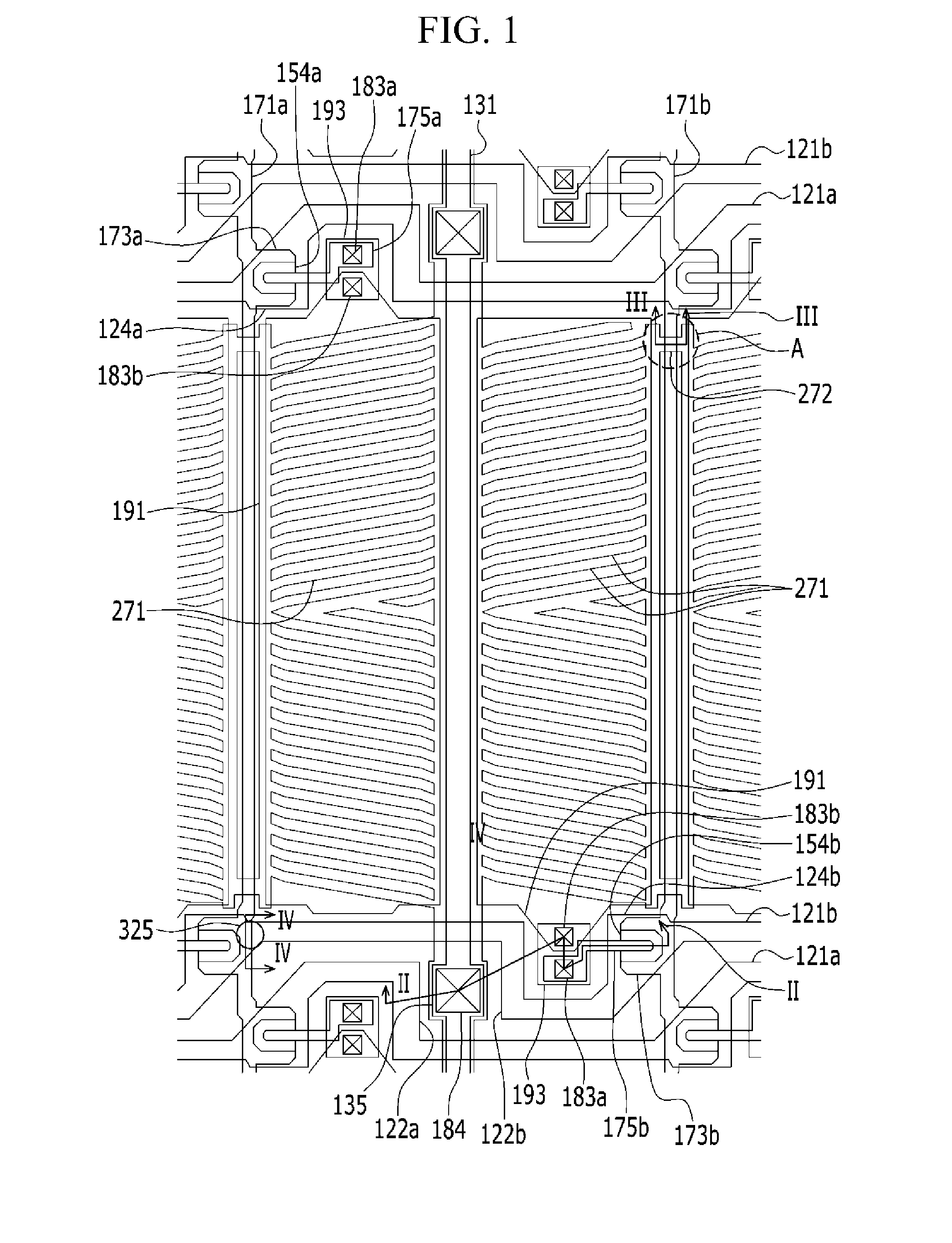
[0016]FIG. 1 is a layout view showing some pixels of a liquid crystal display according to exemplary embodiments of the present invention.

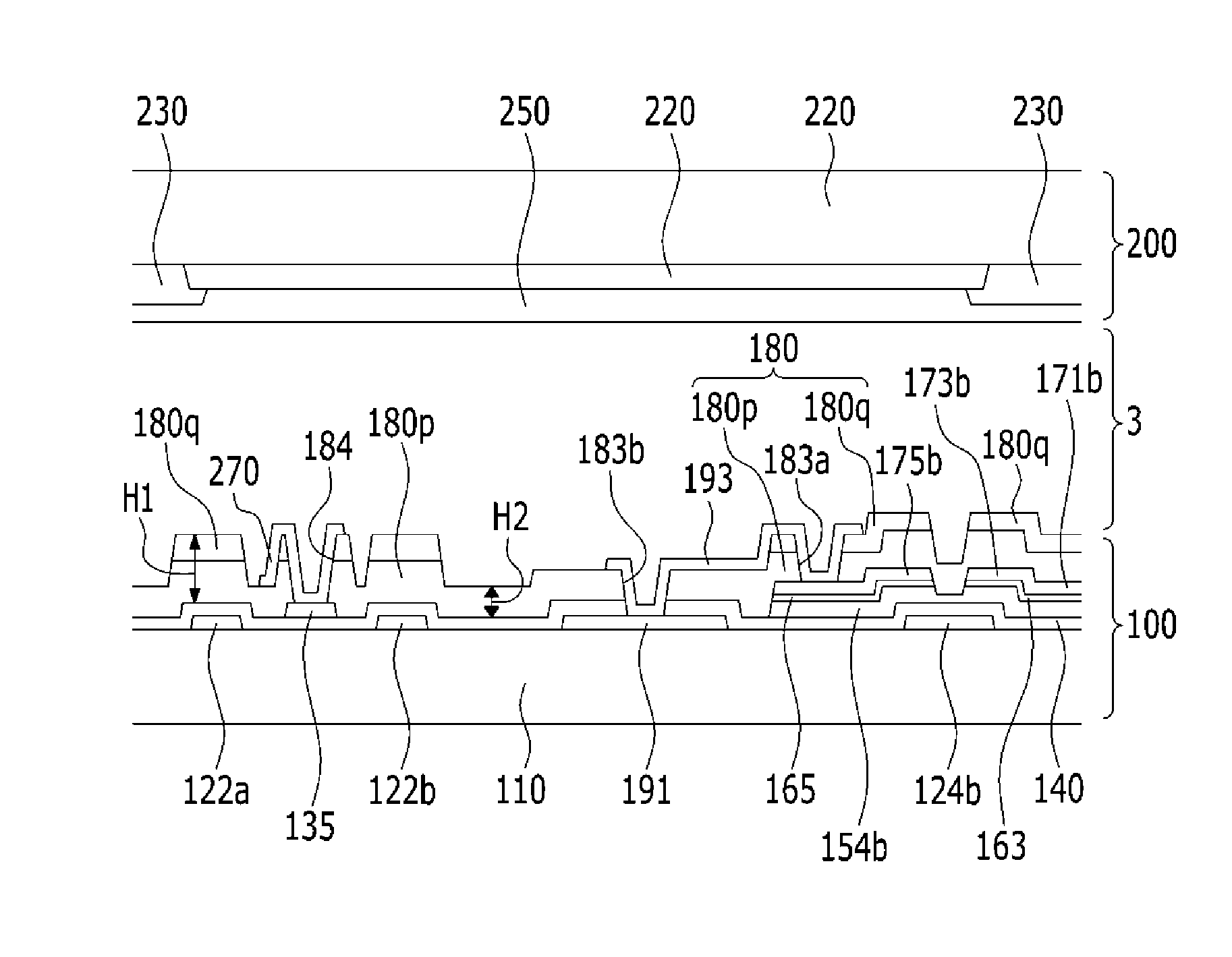
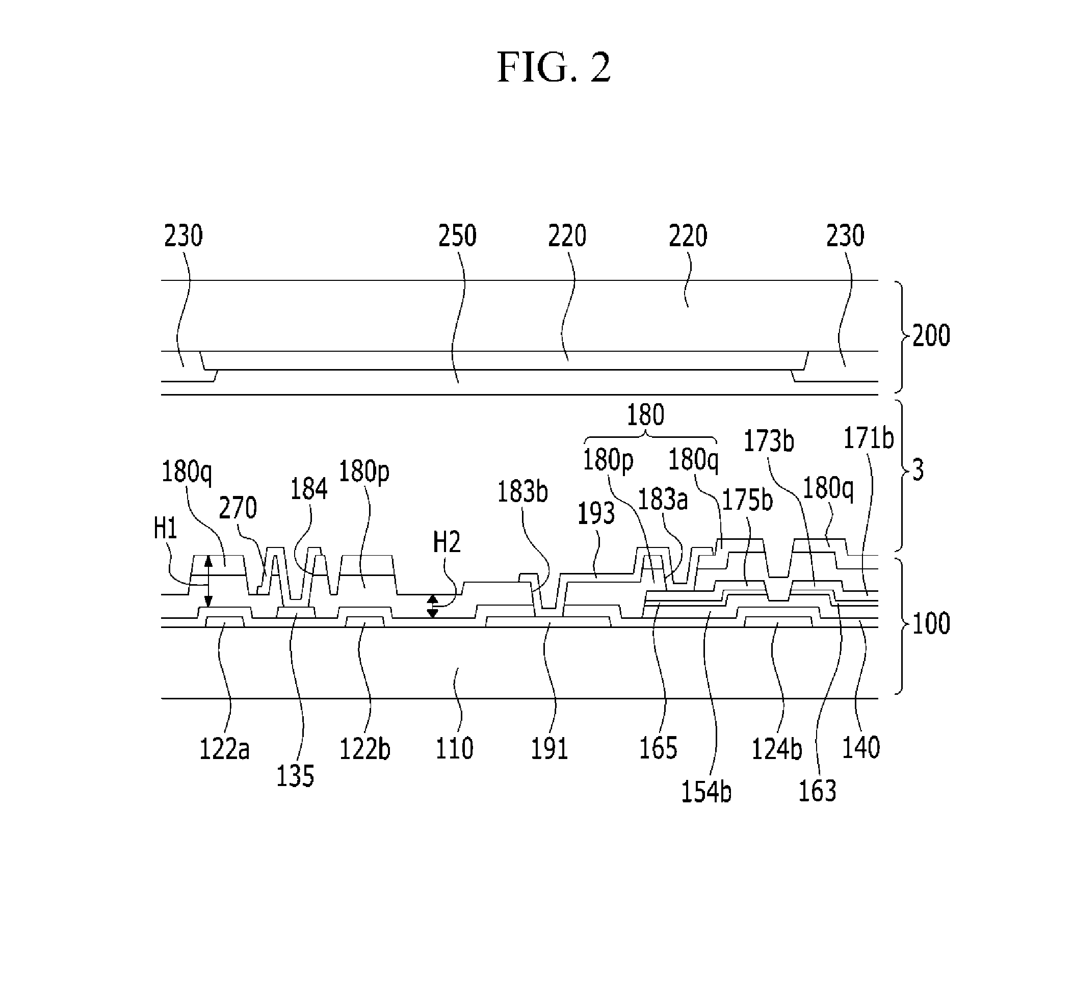
[0017]FIG. 2 is a cross-sectional view taken along line II-II showing the liquid crystal display of FIG. 1.

[0018]FIG. 3 is a cross-sectional view taken along line III-III showing the liquid crystal display of FIG. 1.

[0019]FIG. 4 is a cross-sectional view taken along line IV-IV showing the liquid crystal display of FIG. 1.

[0020]FIG. 5 and FIG. 8 are layout views showing some pixels according to a method of manufacturing a liquid crystal display according to exemplary embodiments of the present invention.

[0021]FIG. 6 is a cross-sectional view taken...


PUM

PropertyMeasurementUnit
thicknessaaaaaaaaaa
photosensitiveaaaaaaaaaa
voltageaaaaaaaaaa

Abstract

In a liquid crystal display (LCD), a thickness of a passivation layer overlapping signal lines is larger than a thickness of portion of the passivation layer not overlapping signal lines. A spacer may be formed to overlap the signal lines. In an aperture region of the LCD, a thickness of the passivation layer between a common electrode and a pixel electrode is relatively small, and therefore, it may be possible to prevent reduction in the intensity of the electric field between the common electrode and the pixel electrode. Since thickness of the passivation layer may be relatively large, it may be possible to prevent a signal delay of common voltage. A spacer may be formed overlapping signal lines with relatively thick passivation layer. The spacer may have a small height. Cell gap may be adjusted to be uniform, and prevent reduction in aperture ratio of the LCD.

Description

CROSS REFERENCE TO RELATED APPLICATION[0001]This application claims priority from and the benefit of Korean Patent Application No. 10-2012-0123210, filed on Nov. 1, 2012, which is hereby incorporated by reference for all purposes as if fully set forth herein.BACKGROUND OF THE INVENTION[0002]1. Field of the Invention[0003]Exemplary embodiments of the present invention relate to a liquid crystal display and a manufacturing method the liquid crystal display.[0004]2. Discussion of the Background[0005]A liquid crystal display, which is one of the most common types of flat panel displays currently in use, is a display device that applies voltage to an electrode to rearrange liquid crystal molecules in a liquid crystal layer so that the amount of light transmitted may be adjusted.[0006]The liquid crystal display has an advantage of having relatively small thickness, but has a drawback in that side visibility is lower compared with front visibility. In order to overcome the drawback, variou...

Claims


Application Information

Patent Timeline
Patent Type & Authority Applications(United States)
IPC IPC(8): G02F1/1333G02F1/1339
CPCG02F1/133345G02F1/1339G02F1/13394G02F1/134363G02F1/136209G02F2201/40G02F1/134372G02F1/1343G02F1/1368
Inventor PARK, GYUNG-SOONKIM, IL GON
Owner SAMSUNG DISPLAY CO LTD
Why Eureka
Try Eureka