Organic light emitting diode display

a light-emitting diode and display technology, applied in static indicating devices, instruments, thermoelectric devices, etc., can solve the problems of deteriorating achieve sufficient laser repair space, reduce the short between driving voltage lines and data lines, and increase the success ratio of laser repair

Active Publication Date: 2014-05-08
SAMSUNG DISPLAY CO LTD
View PDF3 Cites 17 Cited by
  • Summary
  • Abstract
  • Description
  • Claims
  • Application Information

AI Technical Summary

Benefits of technology

[0026]According to the present invention, by forming the partial pixel among a plurality of pixels into the separation pixel in which the driving voltage line is separated in the pixel, the area where the driving voltage line is close to the data line is reduced such that the short between the driving voltage line and the data line is minimized and sufficient

Problems solved by technology

Furthermore, since the interval between the driving voltage line and the data line is very narrow,

Method used


Image

  • Organic light emitting diode display
  • Organic light emitting diode display
  • Organic light emitting diode display

Examples


Embodiment Construction

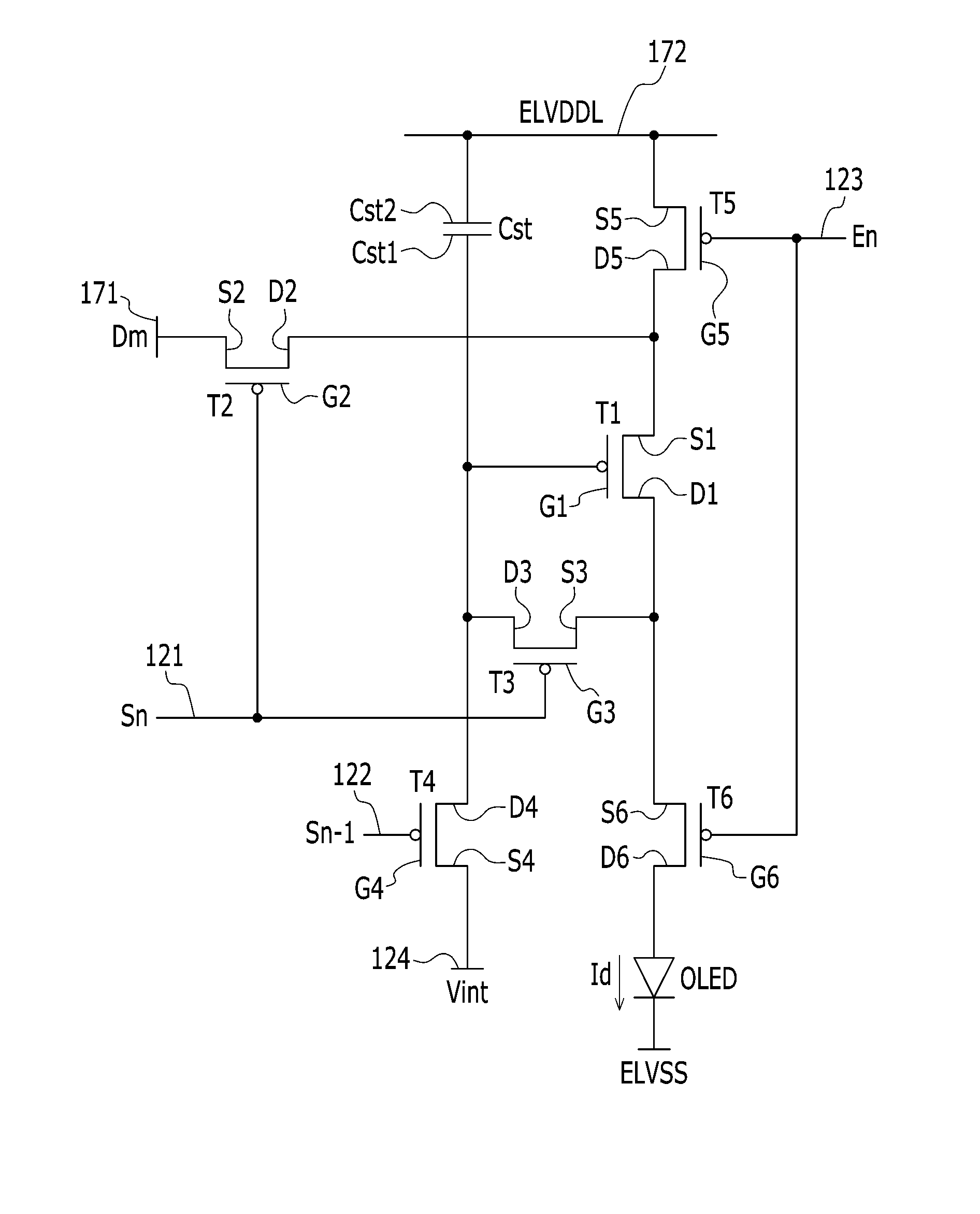
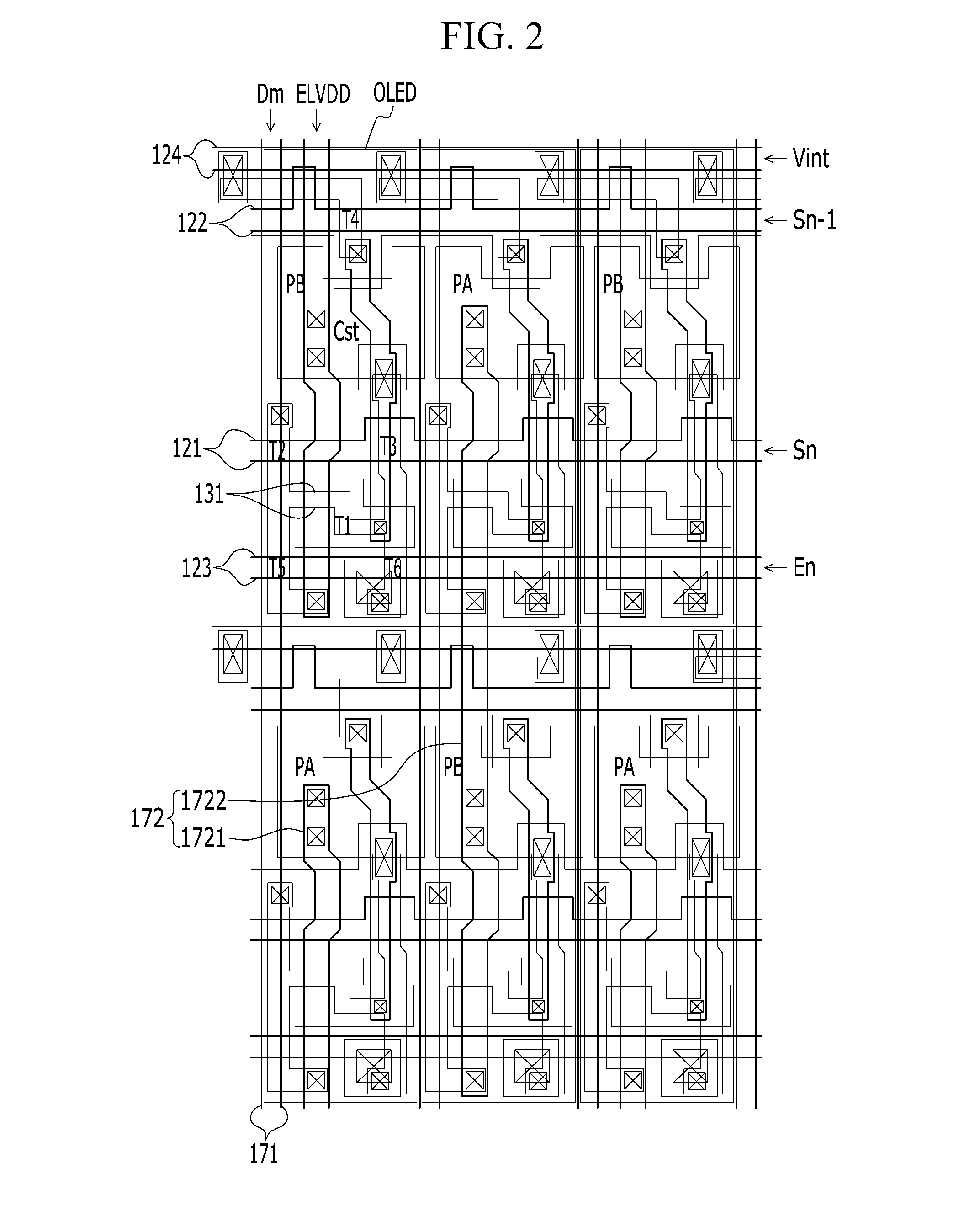
[0037]The present invention will be described more fully hereinafter with reference to the accompanying drawings, in which exemplary embodiments of the invention are shown. As those skilled in the art will realize, the described embodiments may be modified in various different ways, all without departing from the spirit or scope of the present invention.

[0038]In order to clarify the present invention, parts that are not connected with the description will be omitted, and the same elements or equivalents are referred to by the same reference numerals throughout the specification.

[0039]Furthermore, as the size and thickness of the respective structural components shown in the drawings are arbitrarily illustrated for explanatory convenience, the present invention is not necessarily limited to the size and thickness as illustrated.

[0040]In the drawings, the thickness of layers, films, panels, regions, etc. are exaggerated for clarity. In the drawings, for better understanding and ease o...


PUM


Abstract

An organic light emitting diode display according to the present invention includes a substrate and a plurality of pixels formed on the substrate. One pixel includes: a scan line formed on the substrate and transmitting a scan signal; a data line and a driving voltage line crossing the scan line and transmitting a data signal and a driving voltage, respectively; a switching thin film transistor connected to the scan line and the data line; a driving thin film transistor connected to a switching drain electrode of the switching thin film transistor; and an organic light emitting diode connected to a driving drain electrode of the driving thin film transistor. The plurality of pixels includes a separation pixel at which the driving voltage line is separated and a connection pixel at which the driving voltage line is connected.

Description

CLAIM OF PRIORITY[0001]This application makes reference to, incorporates the same herein, and claims all benefits accruing under 35 U.S.C. §119 from an application earlier filed in the Korean Intellectual Property Office filed on 2 Nov. 2012 and there duly assigned Serial No. 10-2012-0123654.BACKGROUND OF THE INVENTION[0002]1. Field of the Invention[0003]The present invention relates generally to an organic light emitting diode (OLED) display.[0004]2. Description of the Related Art[0005]An organic light emitting diode (OLED) display includes two electrodes and an organic emission layer disposed therebetween, electrons injected from one electrode and holes injected from the other electrode are coupled with each other on the organic emission layer to form excitons, and the excitons emit light while emitting energy.[0006]The organic light emitting diode display includes a plurality of pixels including an organic light emitting diode as a self-light emitting element, and each pixel incl...

Claims


Application Information

Patent Timeline
IPC IPC(8): H01L51/52
CPCH01L51/52G09G3/3233G09G2300/0426G09G2300/0819G09G2300/0842G09G2300/0861H10K71/861G09G3/32H10K59/353H10K59/123H10K59/1216H10K59/131
Inventor PARK, KYUNG-MINKIM, TAE-GONKIM, SE-HO
Owner SAMSUNG DISPLAY CO LTD
Why Eureka
Try Eureka