Solution-Processed Metal Selenide Semiconductor using Deposited Selenium Film

Inactive Publication Date: 2014-05-15
SHARP LAB OF AMERICA INC SLA
View PDF14 Cites 0 Cited by
  • Summary
  • Abstract
  • Description
  • Claims
  • Application Information

AI Technical Summary

Benefits of technology

[0031]Disclosed herein is a method to supply additional selenium (Se) to a deposited film of Cu, In, and Ga (CIG) precursors via solution-processing, using a planar Se film that serves as a Se source, upon which subsequent solution-based deposition may be performed. In general, the deposition of Se films can be realized through well-known processing options including chemical bath deposition (CBD), electrochemical deposition, and thermal evaporation, among others. In addition to providing a source of Se from the onset of thermal processing to modulate CIGS films growth, the technology improves interfacial

Problems solved by technology

Unfortunately, most conventional CIGS fabrication strategies require high temperature post-selenization following deposition of the Cu—In—Ga layer.
Even in those cases where selenium is integrated before/during the film deposition stage (as in Se containing nanoparticles or solution based processes with thermally labile Se sources), selenium losses during high temperature processing can render the resultant CIGS film as selenium deficient.
In particular, an inability of the selenium source vapor to penetrate deep into a deposited Cu—In—Ga film can result in reduced grain size, poor overall absorber layer uniformity, and/or morphology as well as poor interfacial contacts, the effects from which are man

Method used


Image

  • Solution-Processed Metal Selenide Semiconductor using Deposited Selenium Film
  • Solution-Processed Metal Selenide Semiconductor using Deposited Selenium Film
  • Solution-Processed Metal Selenide Semiconductor using Deposited Selenium Film

Examples


Embodiment Construction

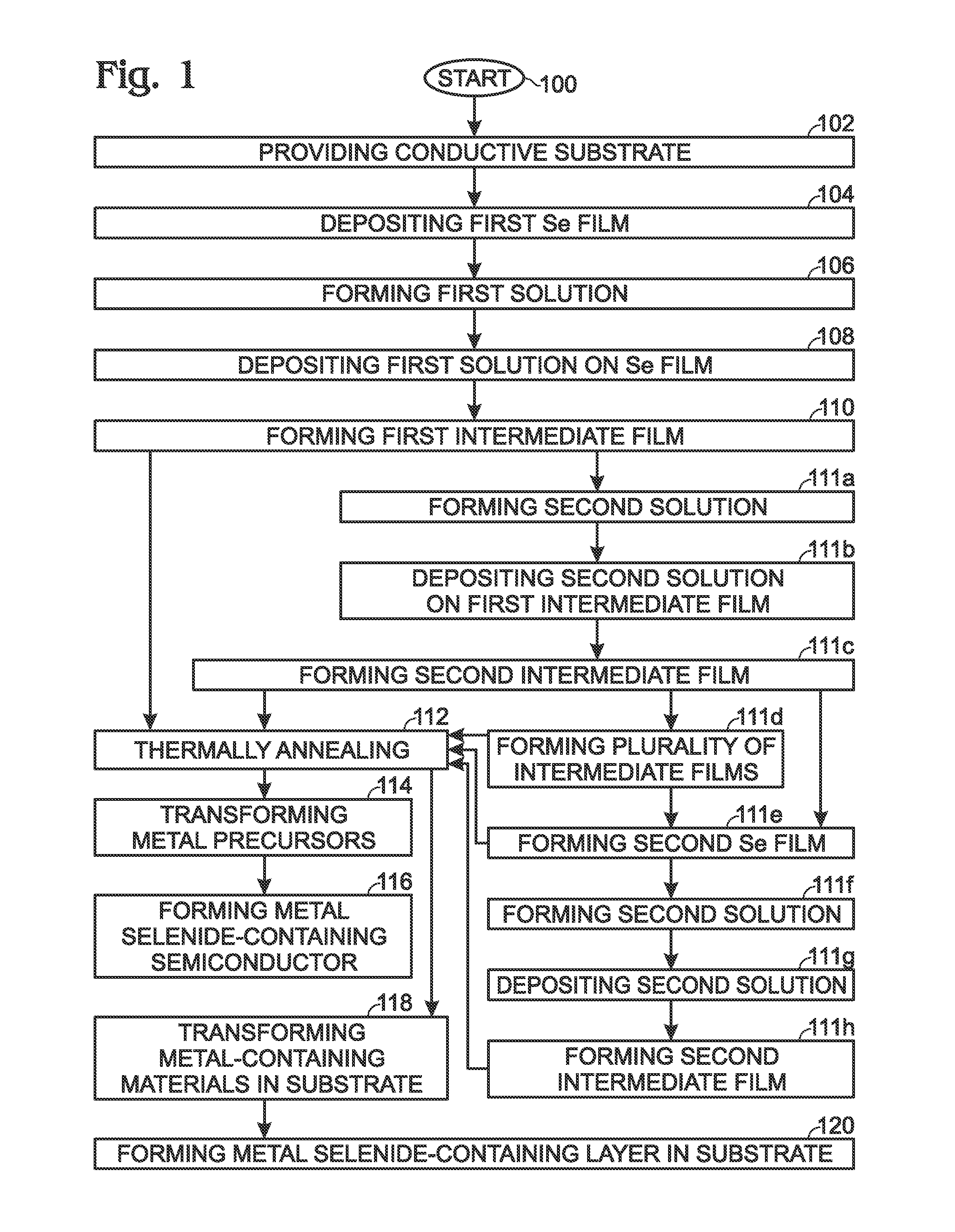
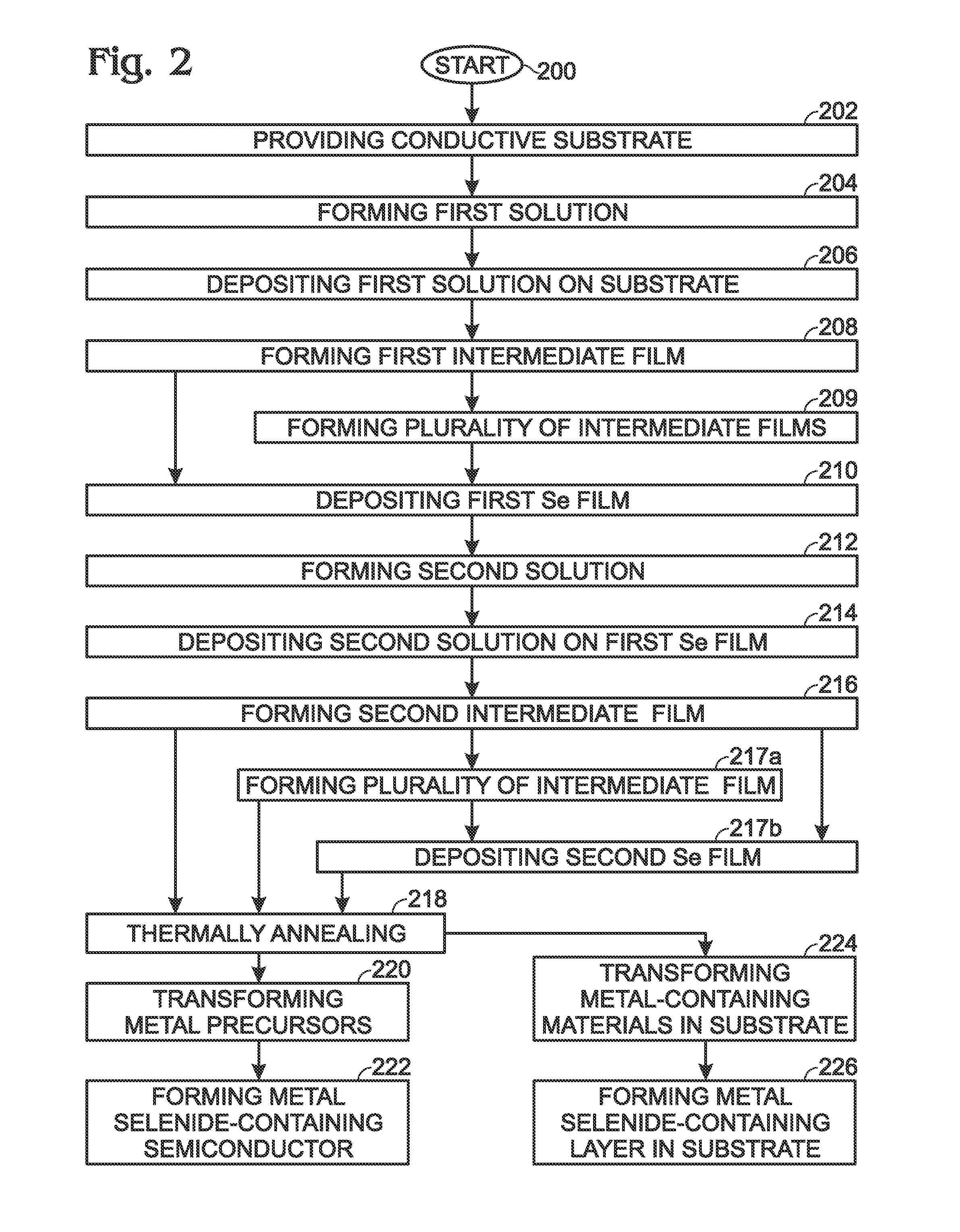
[0043]FIG. 1 is a flowchart illustrating a method for forming a solution-processed metal and mixed-metal selenide semiconductor using a selenium (Se) film layer. Although the method is depicted as a sequence of numbered steps for clarity, the numbering does not necessarily dictate the order of the steps. It should be understood that some of these steps may be skipped, performed in parallel, or performed without the requirement of maintaining a strict order of sequence. Generally however, the method follows the numeric order of the depicted steps. The method begins at Step 100.

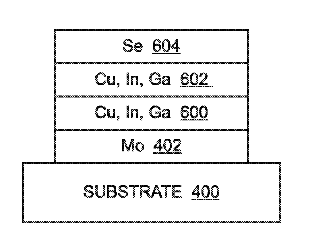
[0044]Step 102 provides a conductive substrate. Step 104 deposits a first Se film layer over the conductive substrate. Step 106 forms a first solution including a first material set of metal salts, metal complexes, and combinations thereof, dissolved in a solvent. Some exemplary members of the first material set include aluminum (Al), antimony (Sb), arsenic (As), bismuth (Bi), cadmium (Cd), cesium (Cs), chromiu...


PUM


Abstract

Methods are provided for fabricating a solution-processed metal and mixed-metal selenide semiconductor using a selenium (Se) film layer. One aspect provides a conductive substrate and deposits a first Se film layer over the conductive substrate. A first solution, including a first material set of metal salts, metal complexes, or combinations thereof, is dissolved in a solvent and deposited on the first Se film layer. A first intermediate film comprising metal precursors is formed from corresponding members of the first material set. In one aspect, a plurality of intermediate films is formed using metal precursors from the first material set or a different material set. In another aspect, a second Se film layer is formed overlying the intermediate film(s). Thermal annealing is performed in an environment including hydrogen (H2), hydrogen selenide (H2Se), or Se/H2. The metal precursors are transformed in the intermediate film(s), and a metal selenide-containing semiconductor is formed.

Description

RELATED APPLICATION[0001]The application is a Continuation-in-Part of an application entitled, ELECTROCHEMICAL SYNTHESIS OF SELENIUM NANOPARTICLES, invented by Wei Pan et al., Ser. No. 13 / 711,356, filed on Dec. 11, 2012, Attorney Docket No. SLA3219;[0002]which is a Continuation-in-Part of an application entitled, SOLUTION-PROCESSED METAL SELENIDE SEMICONDUCTOR USING SELENIUM NANOPARTICLES, invented by Sean Vail et al., Ser. No. 13 / 674,005, filed on Nov. 10, 2012, Attorney Docket No. SLA3211. The above-mentioned applications are incorporated herein by reference.BACKGROUND OF THE INVENTION[0003]1. Field of the Invention[0004]This invention generally relates to metal selenide-containing semiconductors and, more particularly, to processes for forming metal selenide-containing semiconductors using solutions of metal precursors and a deposited Se film layer.[0005]2. Description of the Related Art[0006]Metal and mixed-metal selenides represent important classes of semiconductor materials f...

Claims


Application Information

Patent Timeline
IPC IPC(8): H01L21/02
CPCH01L21/02628H01L21/02491H01L21/02568H01L21/02614H01L31/0322Y02E10/541
Inventor VAIL, SEAN ANDREWKOPOSOV, ALEXEYPAN, WEIFOLEY, GARY D.LEE, JONG-JAN
Owner SHARP LAB OF AMERICA INC SLA
Why Eureka
Try Eureka