Material with steady resistance-vary feature as well as resistance-vary memory

A technology of resistive memory and resistive characteristics is applied in the field of resistive materials, which can solve the problems of unstable resistance value in high and low resistance states, hindering further application of resistive memory, and difficulty in precise control of resistive memory.

Inactive Publication Date: 2008-10-08
PEKING UNIV
View PDF0 Cites 12 Cited by
  • Summary
  • Abstract
  • Description
  • Claims
  • Application Information

AI Technical Summary

Problems solved by technology

The main factor affecting the large-scale application of resistive memory is that the resistance transition conditions of resistive materials are relatively random, and even the pulse conditions for two transitions of the same device often have large deviations.
And in the process of

Method used


Image

  • Material with steady resistance-vary feature as well as resistance-vary memory
  • Material with steady resistance-vary feature as well as resistance-vary memory
  • Material with steady resistance-vary feature as well as resistance-vary memory

Examples


Embodiment Construction

[0023] The preparation of the resistive memory of the present invention will be further described in detail in conjunction with the accompanying drawings:

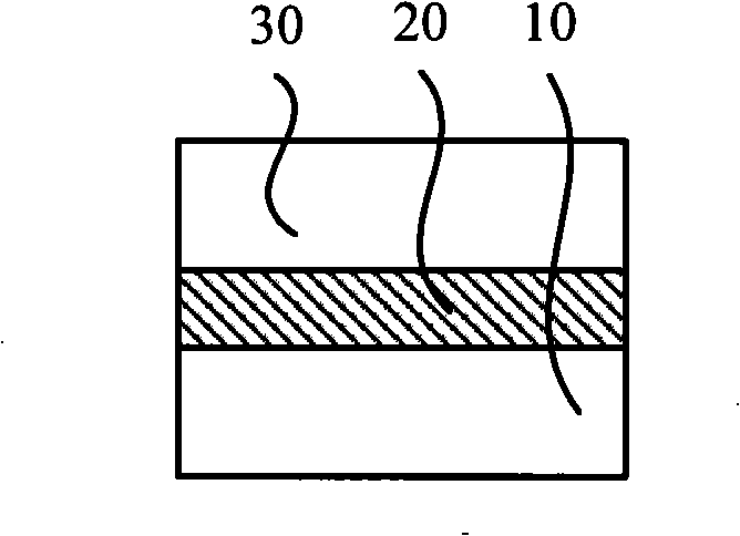
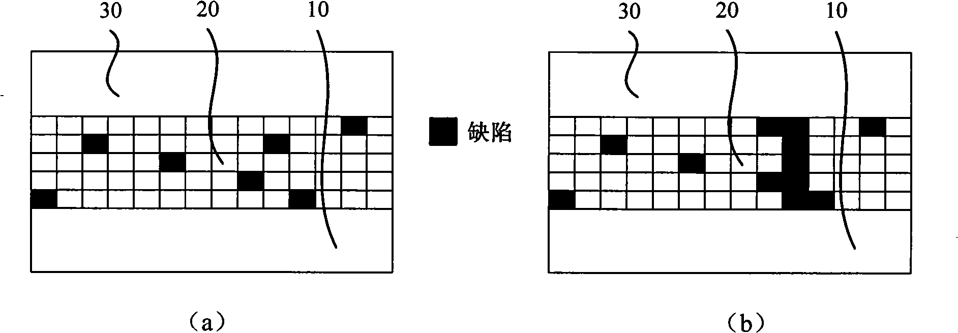
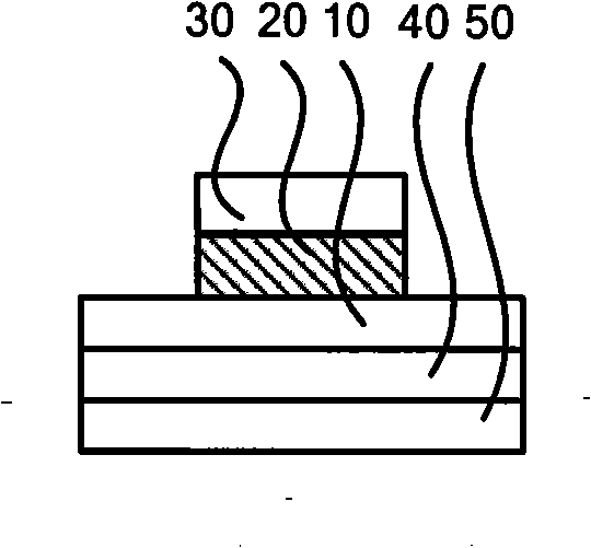
[0024] refer to image 3 , on the SiO on the silicon substrate 50 2 On the insulating medium 40, use PVD (Physical Vapor Deposition) method to grow TiN, HfN or IrO 2 Bottom electrode 10 . On the bottom electrode, grow HfO doped with +3 valent metal element ions by PLD (Pulsed Laser Deposition) method 2 , ZrO 2 or CeO 2 oxide film. The specific manufacturing process is that for PLD to grow doped oxide targets, it is necessary to mix the above-mentioned oxide fine powder and the oxide fine powder of the desired metal element to be mixed evenly, and the above-mentioned mixture is mixed at a temperature of 0.15mbar to 0.25mbar. After being pressed under pressure for 4-8 minutes, it is made by sintering at a high temperature of 900-1200 degrees Celsius for 20-30 hours. The laser power of the PLD is 250mW-350mW, and the d...


PUM

PropertyMeasurementUnit
Thicknessaaaaaaaaaa

Abstract

The invention discloses a material with stable change-resistant capability and a change-resistant memory belonging to field of semiconductor non-volatility memory. The material is an HfO2, ZrO2 or CeO2 thin film doped with metallic element ions of +3 valence. The HfO2, ZrO2 and CeO2 in the change-resistant material have stable lattice structure and less defect state, and Hf, Zr and Ce ions all have +4 valence. Defect can be artificially introduced by doping metallic element ions of +3 valence into the HfO2, ZrO2 and CeO2. So that, HfO2, ZrO2 or CeO2 thin film doped with metallic element ions of +3 valence can be used as change-resistant layer, stability and controllability of change-resistant storage are effectively increased by artificially controlling concentration of defect generation.

Description

technical field [0001] The invention relates to a resistive switch material of a semiconductor non-volatile memory, in particular to a material with stable resistive characteristics and a resistive switch memory. Background technique [0002] Non-volatile memory is a semiconductor storage device that can save information when power is turned off. Non-volatile memories are widely used in current electronic products, such as mobile phones, personal digital assistants (PDAs), and IC cards. The size of semiconductor devices is constantly shrinking, making the design of integrated circuits develop towards system-on-chip (SOC), and a key technology for realizing SOC is the integration of on-chip memory with low power consumption, high density, and fast access speed. The non-volatile memory does not require continuous power supply, making it a natural candidate for large-scale on-chip integrated memory in future SOCs. Since the current mainstream non-volatile memory (floating gat...

Claims


Application Information

Patent Timeline
IPC IPC(8): H01L45/00H01L27/24G11C11/56G11C16/02
Inventor 康晋锋杨竞峰刘力锋孙兵刘晓彦王漪韩汝琦王阳元
Owner PEKING UNIV
Why Eureka
Try Eureka