RF (radio frequency) module and method of maufacturing the same

a technology of radio frequency and module, applied in the field of rf modules, can solve the problems of limiting the degree of freedom of circuit design, difficult to adopt a large number of wirings on the post electrode side, etc., and achieve the effect of ensuring the flexibility of i/o implementation

Inactive Publication Date: 2014-05-29
SAMSUNG ELECTRO MECHANICS CO LTD
View PDF6 Cites 5 Cited by
  • Summary
  • Abstract
  • Description
  • Claims
  • Application Information

AI Technical Summary

Benefits of technology

[0011]An object of the present invention is to provide an RF module capable of designing an IC circuit of a wafer level chip scale package (WLCSP) and a designing an I / O pitch with a sufficient degree of freedom by allowing an RF IC device to perform a function of a main circuit substrate and introducing an auxiliary substrate to secure flexibility of I / O implementation and a method of manufacturing the same.

Problems solved by technology

In a general module technology, a substrate side of a package may adopt a multilayer wiring and a large number of wirings, but a post electrode side is generally difficult to adopt a large number of wirings.
As a result, a degree of freedom of a circuit design may be restricted.

Method used


Image

  • RF (radio frequency) module and method of maufacturing the same
  • RF (radio frequency) module and method of maufacturing the same
  • RF (radio frequency) module and method of maufacturing the same

Examples


Embodiment Construction

[0027]Terms and words used in the present specification and claims are not to be construed as a general or dictionary meaning, but are to be construed to meaning and concepts meeting the technical ideas of the present invention based on a principle that the inventors can appropriately define the concepts of terms in order to describe their own inventions in the best mode.

[0028]Throughout the present specification, unless explicitly described to the contrary, “comprising” any components will be understood to imply the inclusion of other elements rather than the exclusion of any other elements. A term “part”, “ . . . er”“module”, “device”, or the like, described in the specification means a unit of processing at least one function or operation and may be implemented by hardware or software or a combination of hardware and software.

[0029]Hereinafter, exemplary embodiments of the present invention will be described in detail with reference to the accompanying drawings.

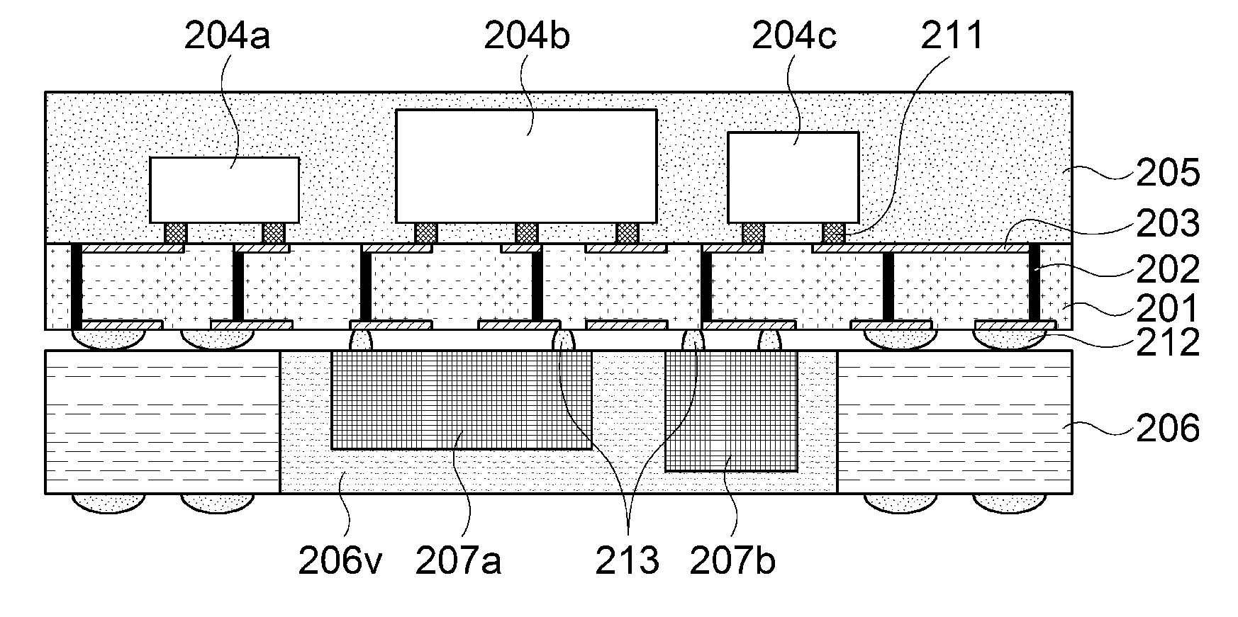
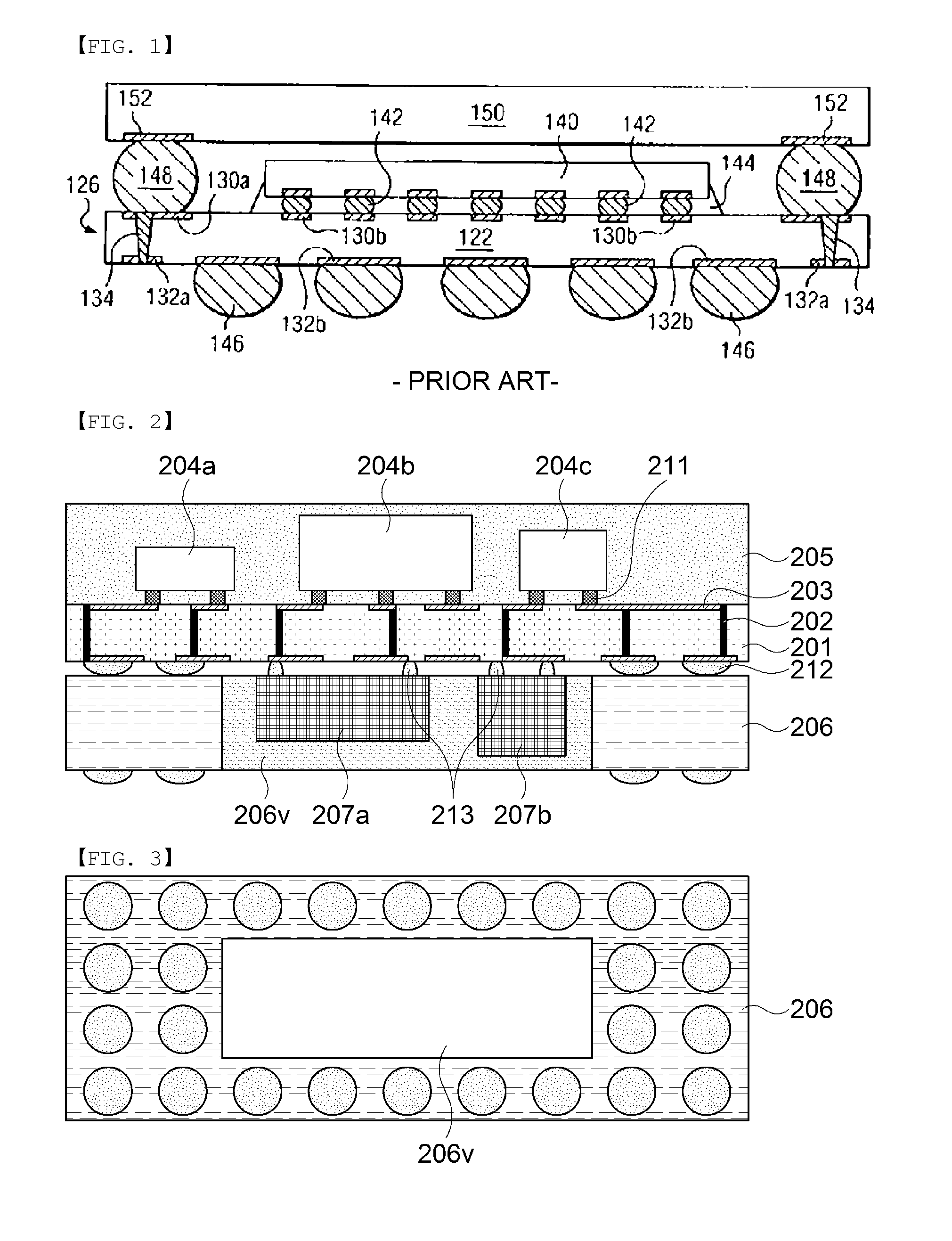
[0030]FIG. 2 is a ...


PUM


Abstract

Disclosed herein are an RF module and a method of manufacturing the same. According to the exemplary embodiment of the present invention, the RF module includes: an RF IC device provided with a via through which upper and lower surfaces thereof are connected to each other; an electronic component mounted on the upper surface or the lower surface of the RF IC device; a molding material having the electronic component sealed therein to protect the electronic component and formed on the upper or lower surface of the RF IC device; and an auxiliary substrate coupled with the upper or lower surface of the RF IC device and providing a place at which other electronic components other than the electronic component sealed in the molding material are mounted, wherein the auxiliary substrate is provided with a through hole having a predetermined size to mount the other electronic components therein.

Description

[0001]This application claims the benefit under 35 U.S.C. Section 119 of Korean Patent Application Serial No. 10-2012-0134455 entitled “RF (Radio Frequency) Module And Method Of Manufacturing The Same” filed on Nov. 26, 2012, which is hereby incorporated by reference in its entirety into this application.BACKGROUND OF THE INVENTION[0002]1. Technical Field[0003]The present invention relates to an RF module and a method of manufacturing the same, and more particularly, to an RF module capable of designing an IC circuit of a wafer level chip scale package (WLCSP) and designing an input / output (I / O) pitch with a sufficient degree of freedom and a method of manufacturing the same.[0004]2. Description of the Related Art[0005]In an RF module which has been used in cellular phones, and the like, a high frequency characteristic is very important. A portion most sensitive to the high frequency characteristics is a wiring between a semiconductor (LSI) chip terminal and external components. Acc...

Claims


Application Information

Patent Timeline
Patent Type & Authority Applications(United States)
IPC IPC(8): H01L25/065H01L23/00
CPCH01L2224/32225H01L2224/73204H01L2924/15311H01L25/50H01L2924/171H01L23/49827H01L21/561H01L24/13H01L24/16H01L24/81H01L2224/16227H01L2924/15331H01L23/13H01L21/486H01L25/0655H01L2224/81192H01L2924/15151H01L2224/16225H01L2924/12042H01L2224/131H01L2924/00H01L2924/014H01L24/95
Inventor CHOI, SEUNG YONG
Owner SAMSUNG ELECTRO MECHANICS CO LTD
Why Eureka
Try Eureka