
Touch electrode device

Active Publication Date: 2014-06-05
HENGHAO TECH CO LTD
View PDF15 Cites 0 Cited by
  • Summary
  • Abstract
  • Description
  • Claims
  • Application Information

AI Technical Summary

Benefits of technology

The present invention aims to provide a touch electrode device with a simplified structure and made of non-transparent conductive material. This would achieve a thinner device and simplify the manufacturing process by directly performing photolithography.

Problems solved by technology

As the ITO is formed by using a complex process and the thickness of each ITO electrode layer is usually between about 100 μm and about 150 μm, so it may cause to increase the overall thickness and result in poor yield for the decorative film.
Consequently, it is difficult to reduce the production costs of the touch panel.

Method used


Image

  • Touch electrode device
  • Touch electrode device
  • Touch electrode device

Examples


Embodiment Construction

[0021]As used in the description herein and throughout the claims that follow, the meaning of “a,”“an” and “the” includes plural reference unless the context clearly dictates otherwise. Also, as used in the description herein and throughout the claims that follow, the meaning of “in” includes “in” and “on” unless the context clearly dictates otherwise.

[0022]As used herein, “around,”“about” or “approximately” shall generally mean within 20 percent, preferably within 10 percent, and more preferably within 5 percent of a given value or range. Numerical quantities given herein are approximate, meaning that the term “around,”“about” or “approximately” can be inferred if not expressly stated.

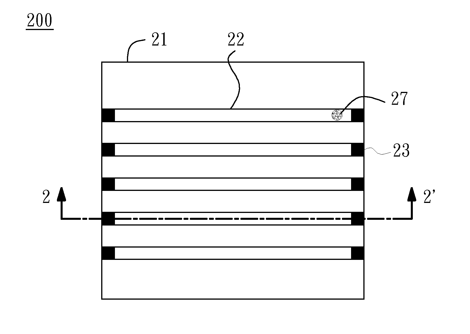
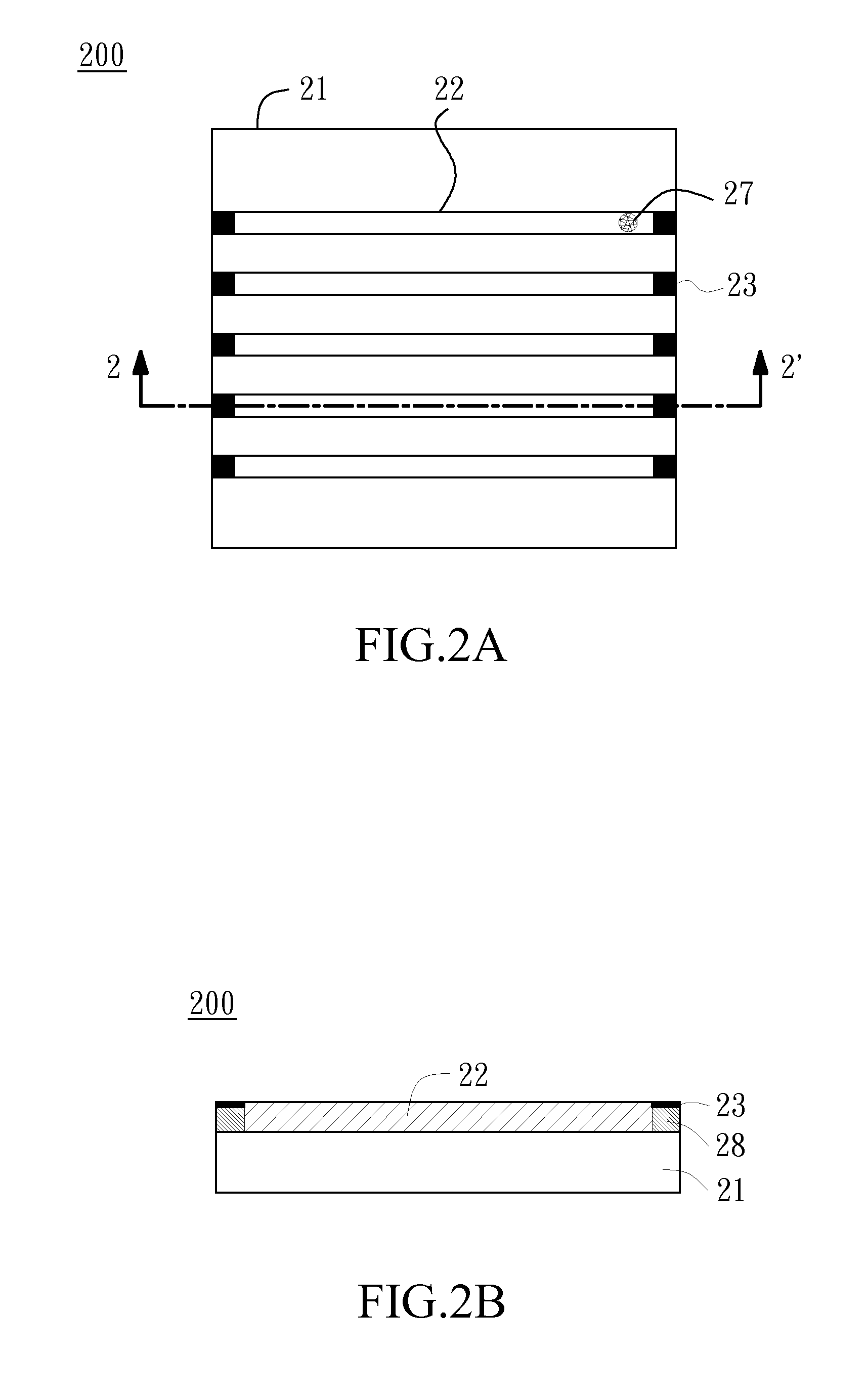
[0023]FIG. 2A shows a top view of a touch electrode device 200 according to one embodiment of the present invention, andFIG. 2B shows a cross-sectional view along a section line 2-2′ in FIG. 2A. Only composing elements pertinent to the embodiment are shown in the figures. The touch electrode device 20...


PUM


Abstract

A touch electrode device includes a substrate, at least one electrode layer and a conductive ink pattern. The electrode layer is disposed above a surface of the substrate, and the electrode layer includes non-transparent conductive material. The conductive ink pattern is printed on two sides of a surface of the electrode layer.

Description

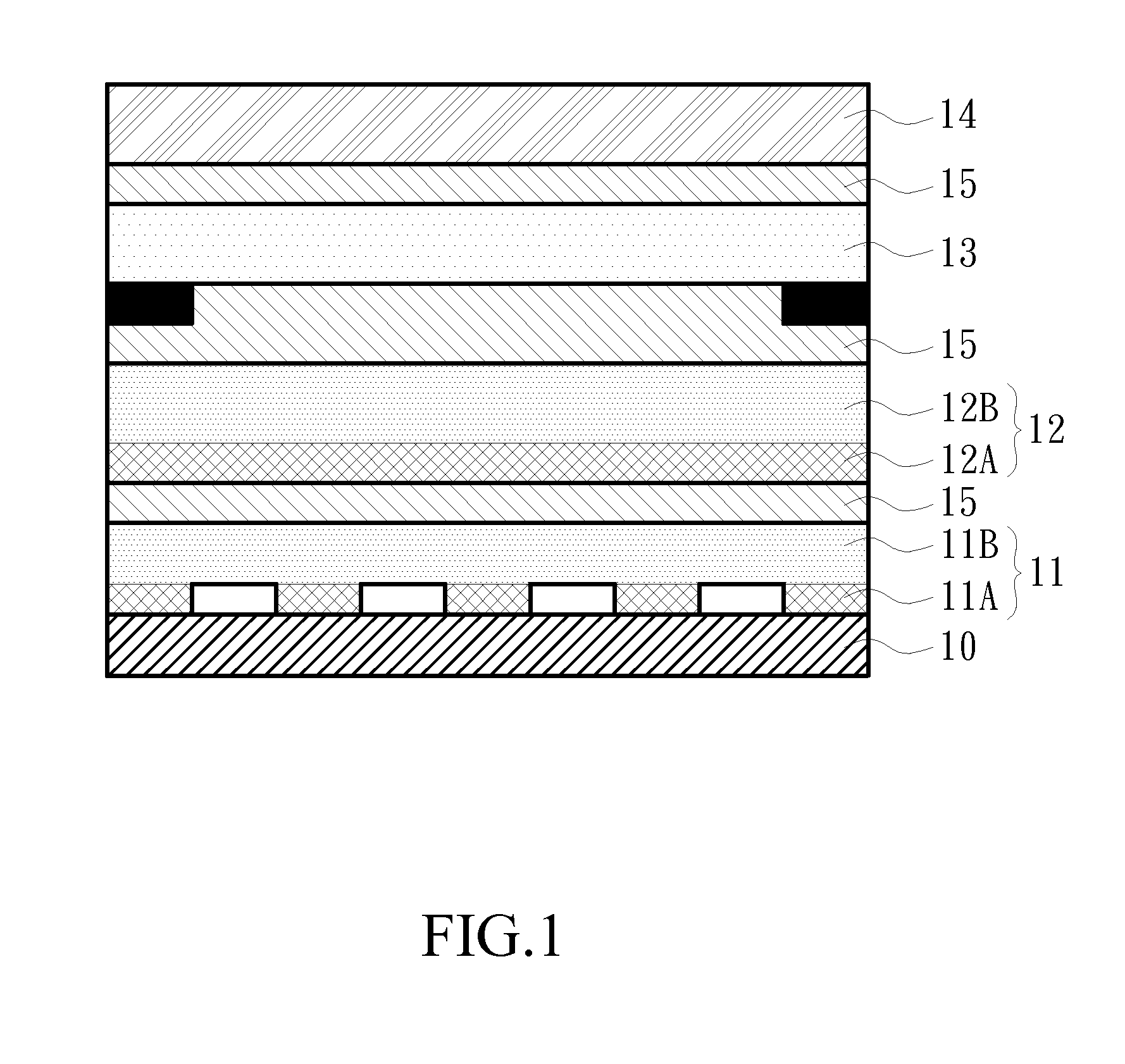
CROSS-REFERENCE TO RELATED APPLICATIONS[0001]The entire contents of Taiwan Patent Application No. 101145014, filed on Nov. 30, 2012, from which this application claims priority, are incorporated herein by reference.BACKGROUND OF THE INVENTION[0002]1. Field of the Invention[0003]The present invention generally relates to a touch electrode device, and more particularly to a touch electrode device having electrodes made up of non-transparent conductive material.[0004]2. Description of Related Art[0005]A touch screen is an input / output device that adopts sensing technology and display technology, and has been widely employed in electronic devices such as portable or hand-held electronic devices.[0006]A capacitor-based touch panel is a commonly used touch panel that utilizes capacitive coupling effect to detect touch position. Specifically, capacitance corresponding to the touch position changes and is thus detected, when a finger touches a surface of the touch panel.[0007]FIG. 1 shows a...

Claims


Application Information

Patent Timeline
IPC IPC(8): H01H1/02
CPCH01H1/02H03K17/962H03K2017/9606H03K2217/960765G06F3/044G06F2203/04103G06F2203/04112
Inventor KUO, YI-PENG
Owner HENGHAO TECH CO LTD
Learn More