Semiconductor module

Active Publication Date: 2014-06-12
MURATA MFG CO LTD
View PDF9 Cites 4 Cited by
  • Summary
  • Abstract
  • Description
  • Claims
  • Application Information

AI Technical Summary

Benefits of technology

The present invention aims to prevent an increase in the size of a communication module that includes a semiconductor module supporting multiple frequency bands. This can be achieved by implementing certain features and techniques described in the patent text.

Problems solved by technology

In other words, a control unit needs to be separately provided in addition to the power amplifier module within a communication module as a unit for power amplification, resulting in an increase in the module size.

Method used


Image

  • Semiconductor module
  • Semiconductor module
  • Semiconductor module

Examples


Embodiment Construction

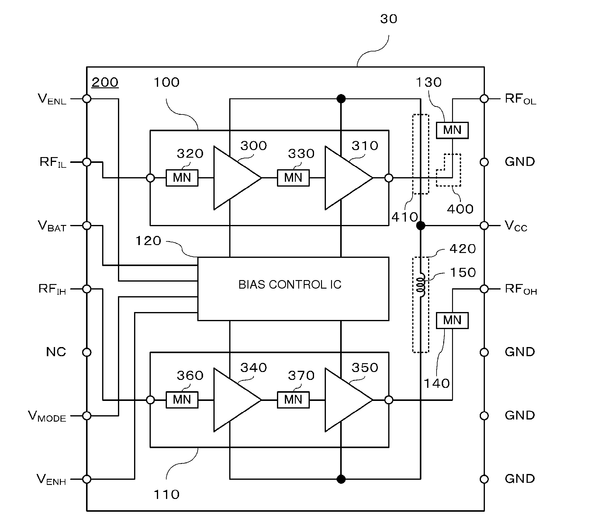
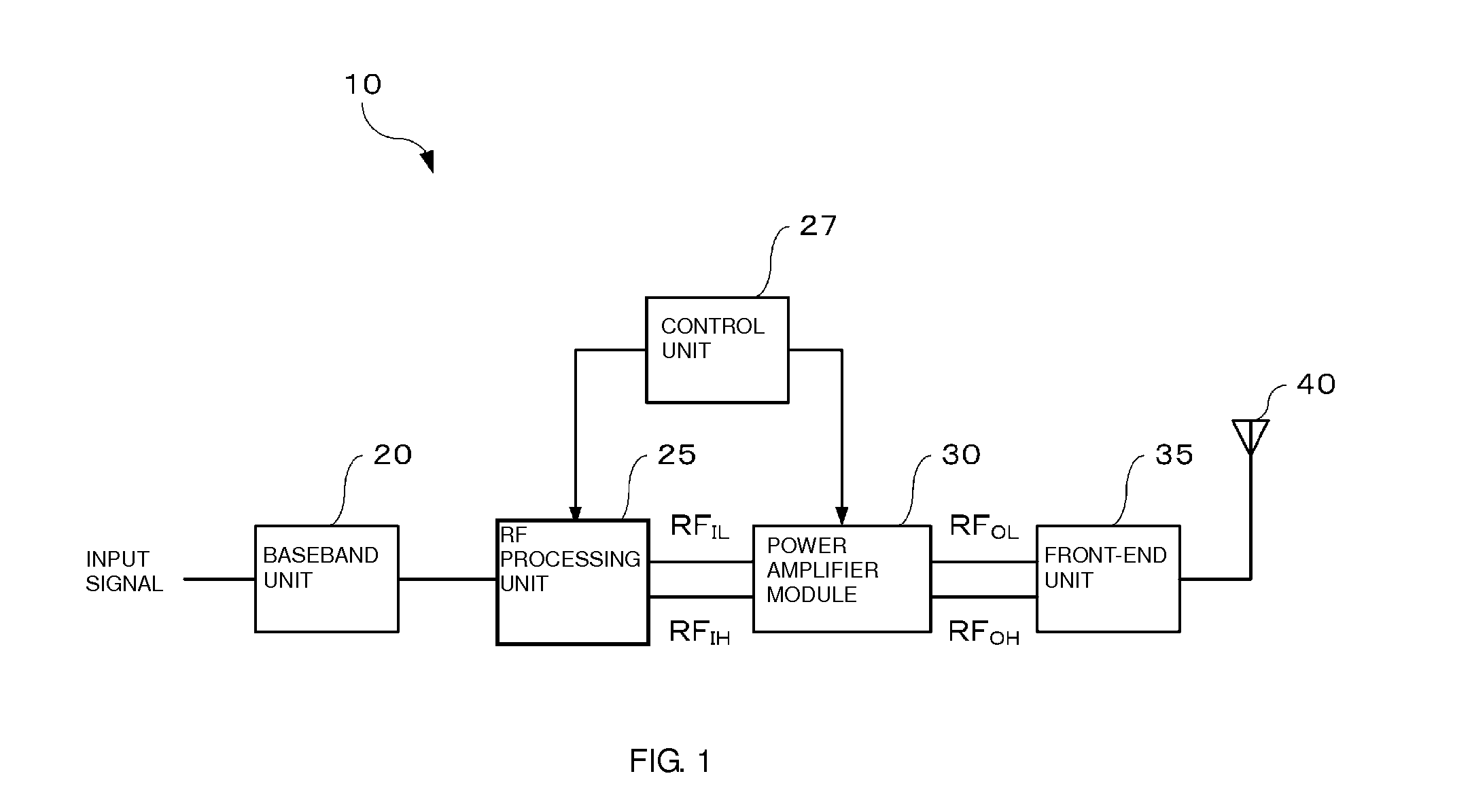
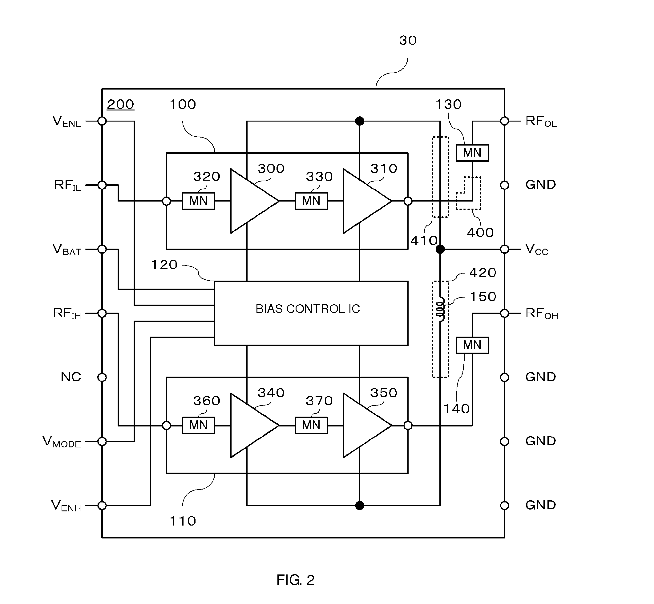
[0015]Hereinafter, preferred embodiments of the present invention will be described with reference to the attached drawings. FIG. 1 is a diagram illustrating an example configuration of a transmission unit including a power amplifier module, which is a preferred embodiment of the present invention. A transmission unit 10 is preferably used, for example, in a mobile communication apparatus, such as a cellular phone, to transmit various signals, such as voice and data, to a base station. Note that although the mobile communication apparatus includes a receiver unit arranged to receive a signal from the base station, description thereof is omitted here.

[0016]Referring to FIG. 1, the transmission unit 10 includes a baseband unit 20, an RF processing unit 25, a control unit 27, a power amplifier module 30, a front-end unit 35, and an antenna 40.

[0017]The baseband unit 20 converts an input signal into an IQ signal and outputs the IQ signal. The RF processing unit 25 modulates an input sig...


PUM


Abstract

A semiconductor module includes a circuit substrate, a first semiconductor device substrate that is mounted on the circuit substrate and that processes an input signal of a first frequency band, a second semiconductor device substrate that is mounted on the circuit substrate and that processes an input signal of a second frequency band, and a control device substrate that is arranged between the first and second semiconductor device substrates and that controls the first and second semiconductor device substrates.

Description

BACKGROUND OF THE INVENTION[0001]1. Field of the Invention[0002]The present invention relates to semiconductor modules.[0003]2. Description of the Related Art[0004]A plurality of frequency bands may be used in wireless communication standards employed by mobile terminals, such as cellular phones. For example, in Global System for Mobile Communications (GSM) (registered trademark), a low-frequency band (for example, 850 MHz band) and a high-frequency band (for example, 1900 MHz) may be used. In order to form a communication module that supports such a plurality of frequency bands, power amplifier modules adapted to respective frequency bands and a switch are required. Hence, a semiconductor module including a plurality of semiconductor device substrates corresponding to respective frequencies are used (for example, Japanese Unexamined Patent Application Publication No. 2006-148268).[0005]The power amplifier module disclosed in Japanese Unexamined Patent Application Publication No. 20...

Claims


Application Information

Patent Timeline
IPC IPC(8): H05K1/18
CPCH05K1/165H03F3/195H03F3/68H03F2200/111H05K1/0228H05K1/0298H05K3/4611H05K2201/09972H05K2201/10015H05K2201/1003H05K2201/10098
Inventor MARUYAMA, MASASHI
Owner MURATA MFG CO LTD
Why Eureka
Try Eureka