
Circuit board and manufacturing method thereof

Inactive Publication Date: 2014-06-26
UNIMICRON TECH CORP
View PDF11 Cites 3 Cited by
  • Summary
  • Abstract
  • Description
  • Claims
  • Application Information

AI Technical Summary

Benefits of technology

The invention is a method of improving the heat dissipating ability of a circuit board by increasing the thickness of the conductive layers that cover the patterned conductive layer and fill the trenches. This is achieved by using a dielectric layer with a specific pattern and a reduced contact area between the circuit layers and dielectric layer, which increases the adhesion force and prevents peeling of the circuit layers. Additionally, the method also reduces the difficulty of filling openings with conductive material in manufacturing processes, resulting in better quality conductive through vias.

Problems solved by technology

However, during the subtractive process, if a conductive layer for forming the circuit layer is too thick, which will lead to a long time to etch, and an etching solution will accumulate to form a pond between circuit patterns and influence etching capability.
In addition, during the etching process, if the conductive layer is too thick, usually a longer etching time is needed, which consequently makes the etching solution cause a serious lateral etching effect on the side walls of a circuit pattern, affecting the quality and reliability of a circuit, and also is disadvantageous for manufacture of a fine circuit.
On the other hand, if the thickness of the conductive layer is decreased for avoiding the above problems, the thermal capacity of a formed structure will be consequently inadequate and thus a good heat dissipating capability cannot be provided.
However, after etching is performed, usually the surface of the dielectric layer in the trench is easily exposed, which consequently affects follow-up processes.
Additionally, when a semi-additive process (SAP) is used for manufacturing a fine circuit, the contact area between a circuit and a dielectric layer is often too small, which results in the fine circuit having inadequate peeling strength and easily being peeled from the dielectric layer, therefore decreasing the reliability of a circuit board.
However, in the process of filling the opening with the conductive material layer, an aspect ratio of the opening is usually too big, which makes it uneasy to fill the conductive material in.

Method used


Image

  • Circuit board and manufacturing method thereof
  • Circuit board and manufacturing method thereof
  • Circuit board and manufacturing method thereof

Examples


Embodiment Construction

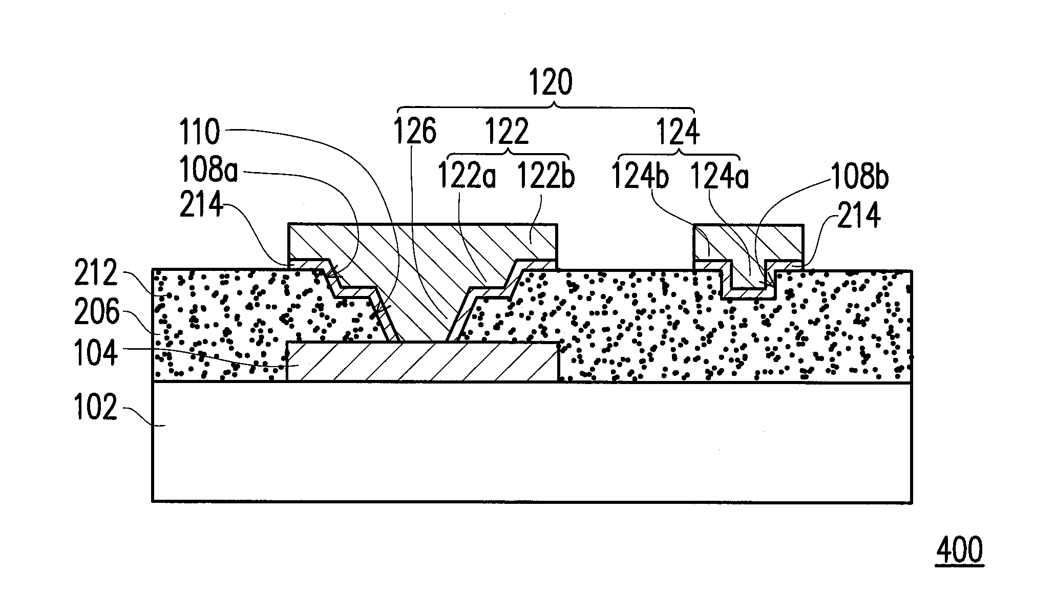
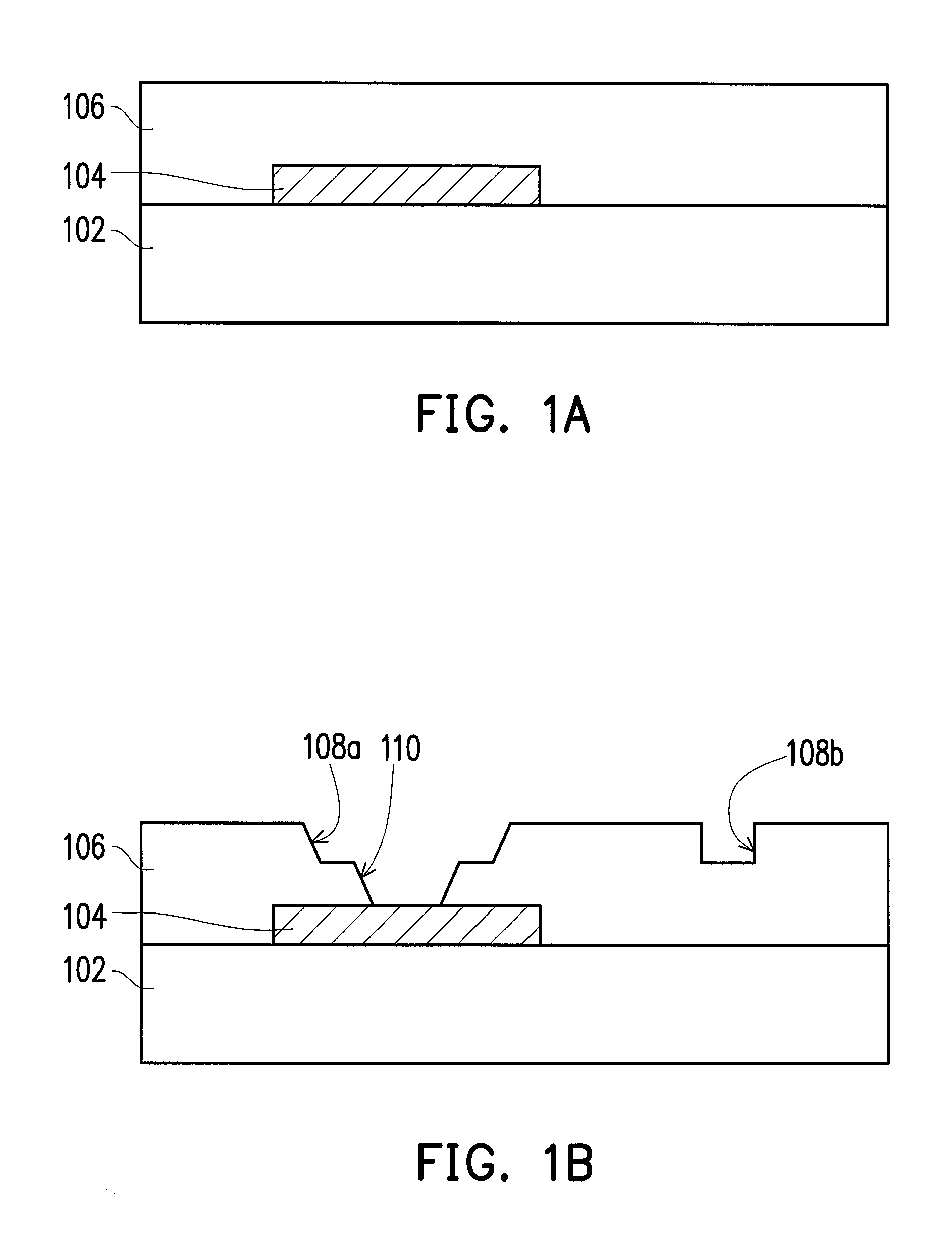
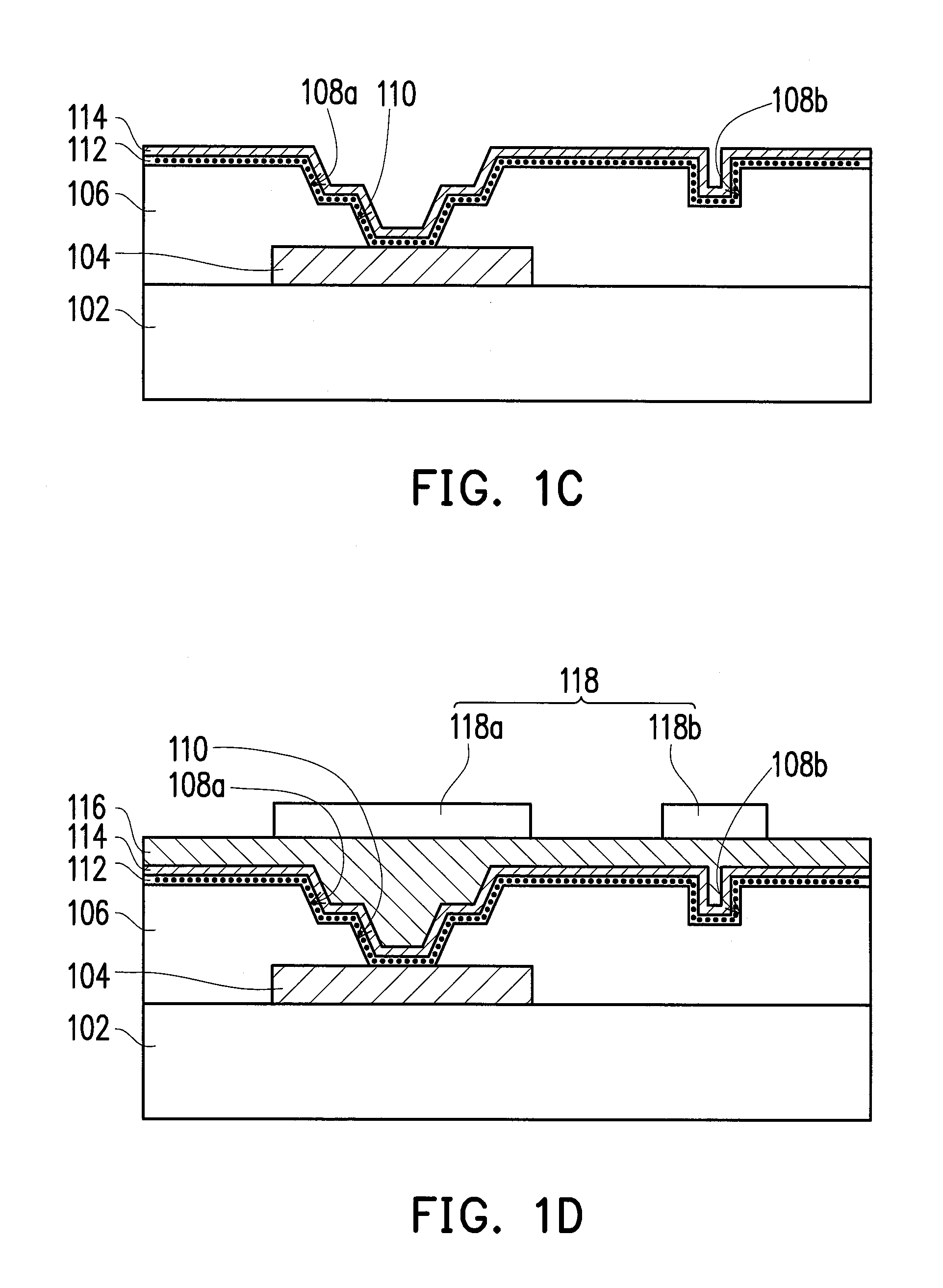
[0031]FIGS. 1A-1E are cross-sectional schematic drawings showing a manufacturing method of a circuit board illustrated according to the first embodiment of the present invention. Firstly, please refer to FIG. 1A, a dielectric layer 106 is formed on a substrate 102. The substrate 102 is, for example, a dielectric substrate. Besides, the substrate 102 has an internal circuit layer 104 formed thereon. The dielectric layer 106 covers the substrate 102 and the internal circuit layer 104. A material of the dielectric layer 106 is, for example, polypropylene (PP), polyimide (PI), Ajinomoto build-up film or liquid crystal polymer (LCP).

[0032]Then, please refer to FIG. 1B, a first trench 108a, a second trench 108b and an opening 110 are formed in the dielectric layer 106, wherein the opening 110 is located below the first trench 108a and connected with the first trench 108a. Besides, a portion of the internal circuit layer 104 is exposed by the opening 110. The first trench 108a, the second ...


PUM

PropertyMeasurementUnit
Electrical conductoraaaaaaaaaa

Abstract

A circuit board and a manufacturing method thereof are provided. A dielectric layer is formed on a substrate, wherein an internal circuit layer is formed on the substrate and the dielectric layer covers the internal circuit layer. A first trench, a second trench and an opening are formed in the dielectric layer. The opening is located below the first trench and connected with the first trench, and a portion of the internal circuit layer is exposed by the opening. A patterned conductive layer is formed on the dielectric layer. The patterned conductive layer covers a portion of the dielectric layer and fills the first trench, the second trench and the opening so as to form a first circuit layer, a second circuit layer and a conductive through via, respectively, wherein the conductive through via is electrically connected with the first circuit layer and the internal circuit layer.

Description

BACKGROUND OF THE INVENTION[0001]1. Field of the Invention[0002]The invention relates to a circuit board and a manufacturing method thereof, and in particular relates to a circuit board having both an embedded circuit layer and a surface circuit layer, and a manufacturing method thereof.[0003]2. Description of Related Art[0004]For the past few years, with rapid development of electronic technologies and high tech electronics industries being introduced, electronic products that are more humanized and with better functions have been continuously launched, and have been designed to be small, slim and lightweight. These electronic products are usually equipped with a circuit board with a conductive circuit.[0005]In general, a subtractive process can be used to manufacture a circuit layer in a circuit board when manufacturing the circuit board. However, during the subtractive process, if a conductive layer for forming the circuit layer is too thick, which will lead to a long time to etc...

Claims


Application Information

Patent Timeline
IPC IPC(8): H05K3/06H05K1/02
CPCH05K3/06H05K3/108H05K3/465H05K2203/0723
Inventor YU, CHENG-POHUANG, HAN-PEIHUANG, SHANG-FENG
Owner UNIMICRON TECH CORP
Learn More