
Charged particle beam apparatus

a particle beam and apparatus technology, applied in the direction of material analysis using wave/particle radiation, instruments, nuclear engineering, etc., can solve the problems of difficult to detect the energy distribution, large device size and cost, and inapplicability, so as to improve the elucidation of physical phenomena and easy discrimination of angles and energy of the se

Inactive Publication Date: 2014-06-26
HITACHI HIGH-TECH CORP
View PDF3 Cites 26 Cited by
  • Summary
  • Abstract
  • Description
  • Claims
  • Application Information

AI Technical Summary

Benefits of technology

The present invention provides an SEM device that can easily discriminate the angles and energy of the SE or BSE for imaging. This device can visualize the necessary information on a sample to be observed and improve physical phenomenon elucidation of the sample. Additionally, the device is convenient and can discriminate the SE or BSE with a specific energy or energy that is settable.

Problems solved by technology

It is very difficult to detect the energy distribution while changing a threshold on a higher energy side of the energy distributions of the SE and the BSE.
However, the device is massive and expensive, and not applied in the marketed conventional SEM.

Method used


Image

  • Charged particle beam apparatus
  • Charged particle beam apparatus
  • Charged particle beam apparatus

Examples


Embodiment Construction

[0030]Hereinafter, embodiments will be described with reference to the drawings.

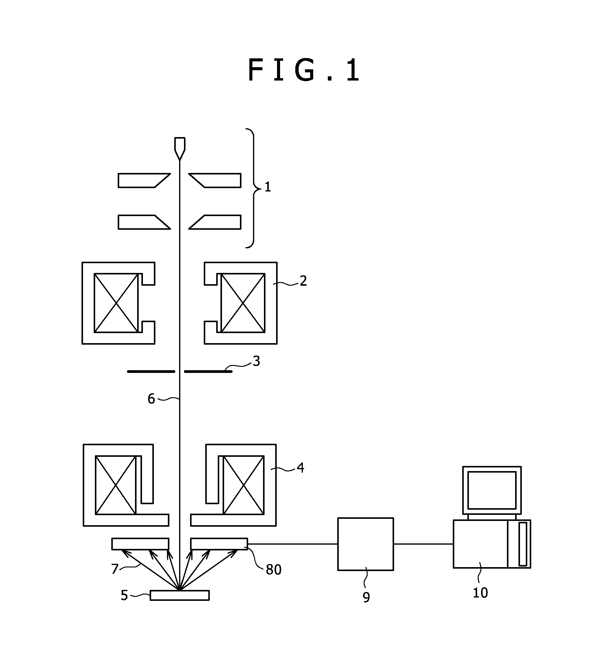
[0031]FIG. 1 is a schematic view of a scanning electron microscope (SEM) according to the present invention.

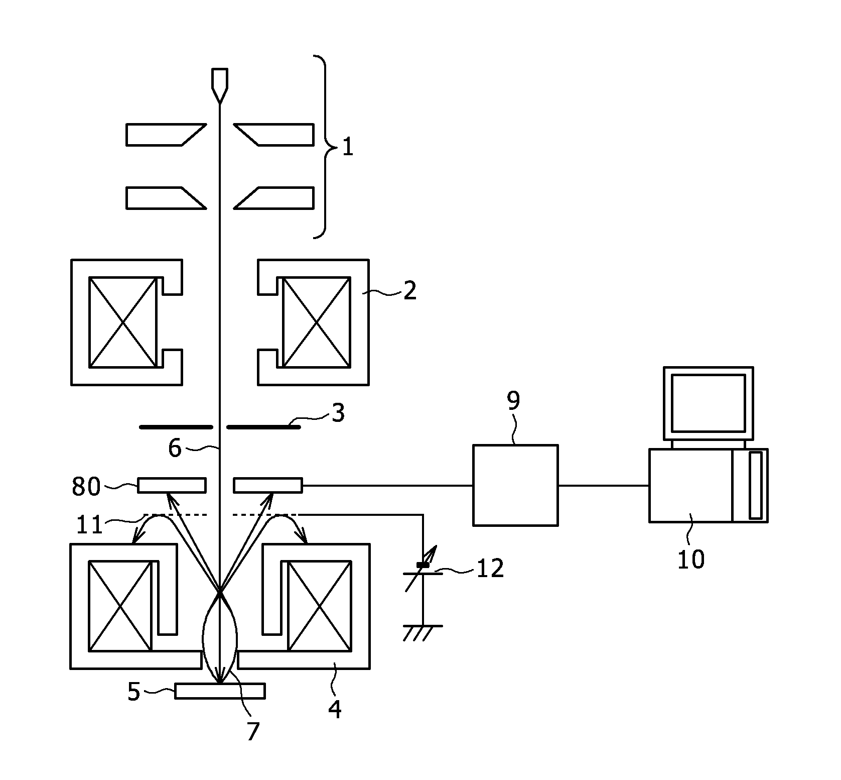
[0032]An electron gun 1 takes a primary electron beam 6 from an electron source, and accelerates the primary electron beam 6 up to an energy set by a user. A condenser lens 2 controls a probe current quantity of the primary electron beam 6 and a convergence angle of the primary electron beam 6 to a sample according to a relationship with an aperture 3 or an objective lens 4. The objective lens 4 focuses the primary electron beam 6 on a sample 5. When the sample 5 is irradiated with the primary electron beam 6, emitted electrons 7 are emitted depending on an energy thereof at the time of irradiation, and a composition, a crystalline property, a sample voltage potential, a topographic property, a sample thickness, and a sample inclined angle (convergence angle of the primary electron beam 6 to the sa...


PUM


Abstract

A charged particle beam apparatus that easily discriminates the angles and energy of the SE or the BSE, and images information necessary for a sample to be observed.The charged particle beam apparatus having a charged particle source that emits a primary charged particle beam, a condenser lens that condenses the primary charged particle beam on a sample, and a detector that detects secondary charged particles emitted from a radiated point on the sample, the charged particle beam apparatus including: a pulse processing unit that subjects a signal from the detector to pulse processing, and creates energy distribution information of the secondary charged particles; and a control unit that selects information in an arbitrary energy region of the energy distribution information, and display an image on a display unit.

Description

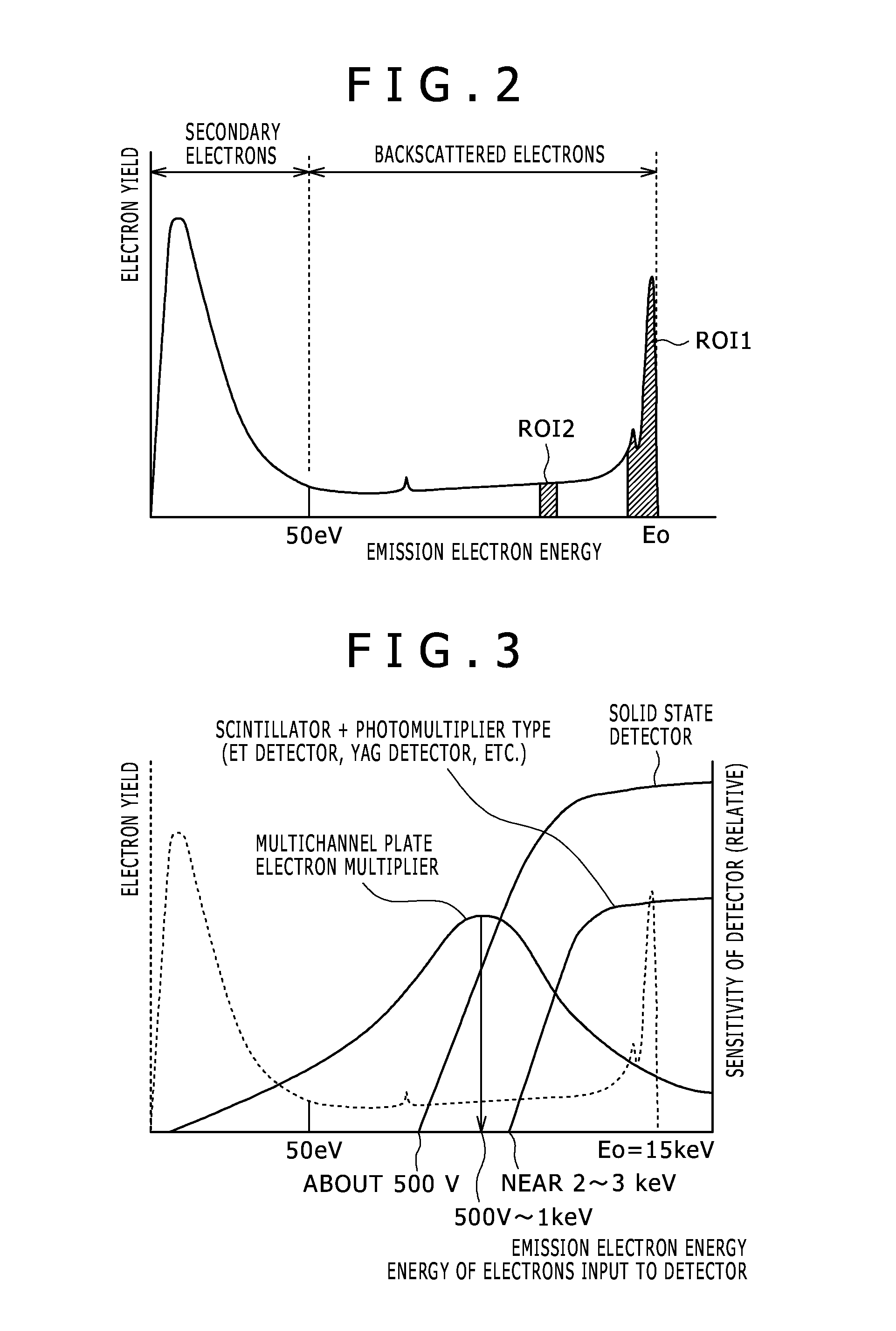
TECHNICAL FIELD[0001]The present invention relates to a charged particle beam apparatus, and more particularly to a detector and a detecting method for secondary charged particles in a charged particle beam apparatus for observing a sample through a scanning electron beam.BACKGROUND ART[0002]In recent years, scanning electron microscopes (SEM) have been used to observe a surface or a cross-section of target samples in extensive fields. The SEM detects secondary electrons (SE) having a relatively low energy of 0 to 50 eV, which are generated by an interaction of a primary electron beam and the sample, and backscattered electrons (BSE) having an extensive distribution from 50 eV to an energy of the primary electron beam for imaging.[0003]There has been generally known that obtained information is different according to respective energy regions detected by the SE and the BSE. For example, SE having several of eV reflects sample surface or topographic information, and the SE having a m...

Claims


Application Information

Patent Timeline
Patent Type & Authority Applications(United States)
IPC IPC(8): H01J37/244H01J37/28
CPCH01J37/28H01J37/244H01J37/222H01J2237/2445
Inventor AGEMURA, TOSHIHIDE
Owner HITACHI HIGH-TECH CORP
Learn More