
Nonvolatile memory device and method for fabricating the same

Active Publication Date: 2014-06-26
SK HYNIX INC
View PDF2 Cites 57 Cited by
  • Summary
  • Abstract
  • Description
  • Claims
  • Application Information

AI Technical Summary

Benefits of technology

This patent is about two different types of memory devices that have certain benefits. One device can prevent over-erasing, which means it can protect information from being accidentally deleted. Another device can reduce the amount of power needed to operate it. The patent describes how these benefits can be achieved and how they can be used in practical applications.

Problems solved by technology

If a system design technology is not secured, it may be difficult to develop non-memory semiconductors.
In the flash memory device having the above structure, a problem may be caused in that over-erase is likely to occur in an erase operation.
Further, while the conventional flash memory device uses a hot carrier injection (HCI) scheme for a program operation, since the HCI scheme consumes a large amount of current for programming, the HCI scheme is inappropriate for an embedded memory.

Method used


Image

  • Nonvolatile memory device and method for fabricating the same
  • Nonvolatile memory device and method for fabricating the same
  • Nonvolatile memory device and method for fabricating the same

Examples


first embodiment

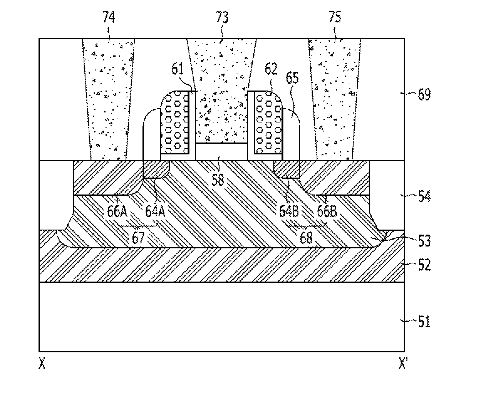
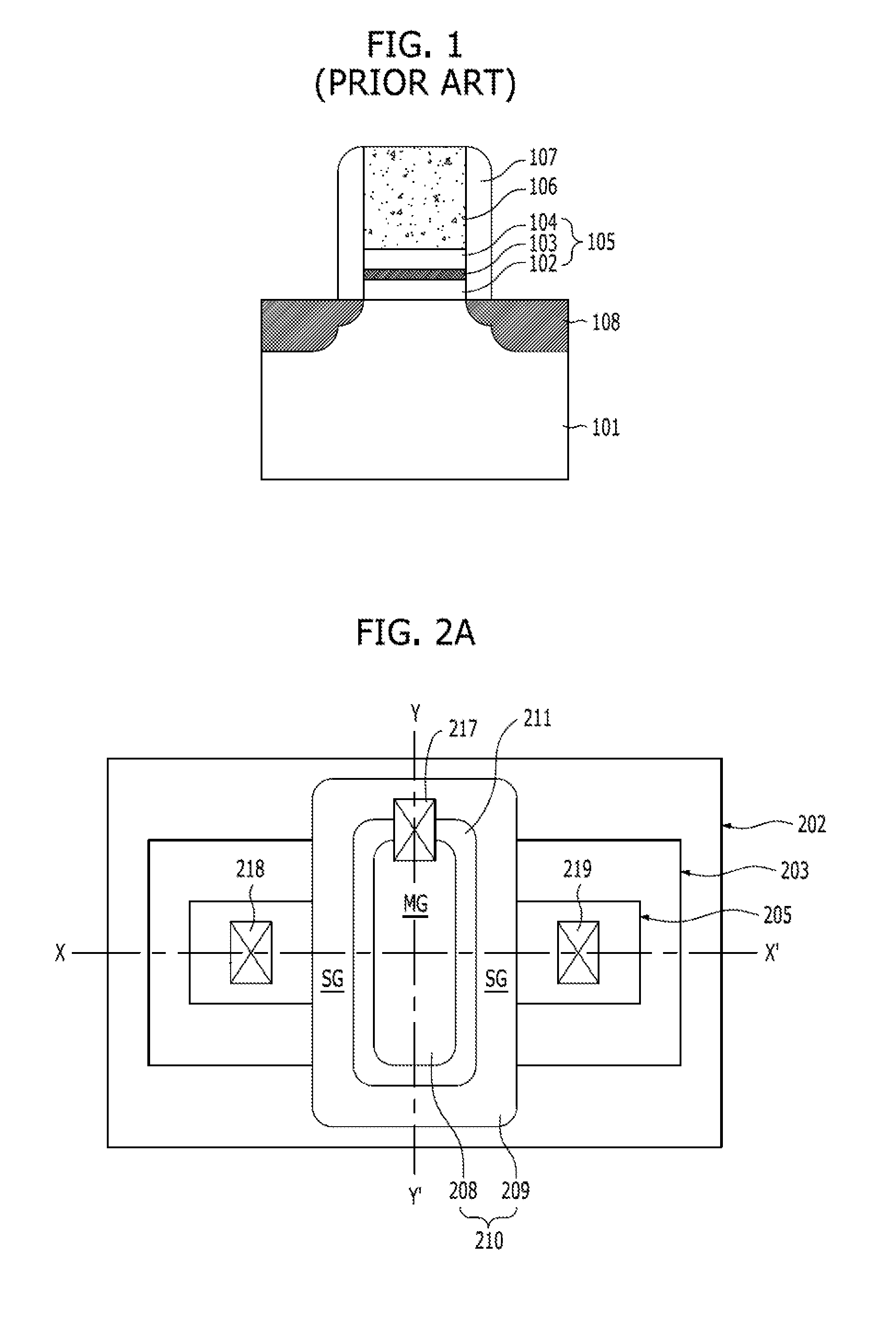
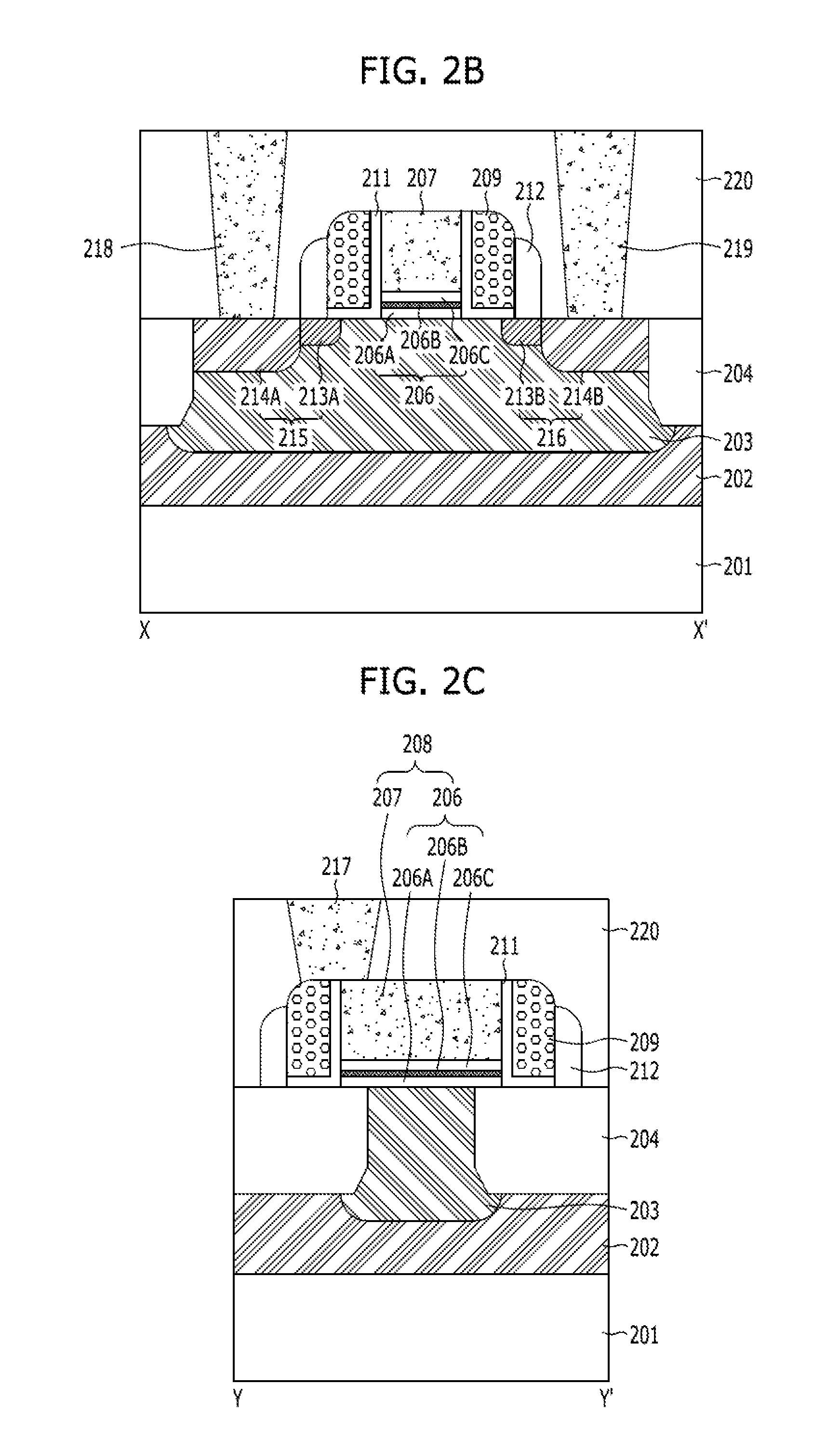
[0031]FIGS. 2A to 2C are views illustrating a nonvolatile memory device in accordance with a In detail, each of FIGS. 2A to 2C illustrates a unit cell of the nonvolatile memory device, wherein FIG. 2A is a plan view and FIGS. 2B and 2C are cross-sectional views taken along the lines X-X′ and Y-Y′ of FIG. 2A.

[0032]Referring to FIGS. 2A to 2C, a nonvolatile memory device in accordance with a first embodiment includes a memory gate (MG) 208 in which a memory layer 206 and a gate electrode 207 are stacked on a substrate 201, a select gate (SG) 209 which is formed on sidewalls of the memory gate 208, a source region 215 and a drain region 216 which are formed in the substrate 201 on sides of a gate pattern 210 including the memory gate 208 and the select gate 209, and a gate contact 217 which electrically connects the memory gate 208 to the select gate 209.

[0033]A deep well 202 of the second conductivity type and an isolated well (or isolation well) 203 of the first conductivity type (o...

second embodiment

[0075]FIGS. 5A to 5C are views illustrating a nonvolatile memory device in accordance with a In detail, FIGS. 5A to 5C illustrate a unit cell of the nonvolatile memory device, wherein FIG. 5A is a plan view and FIGS. 5B and 5C are cross-sectional views taken along the lines X-X′ and Y-Y′ of FIG. 5A, respectively.

[0076]Referring to FIGS. 5A to 5C, a nonvolatile memory device in accordance with the second embodiment includes a memory gate (MG) 308 in which a memory layer 306 and a gate electrode 307 are stacked on a substrate 301, a select gate (SG) 309 which is formed on sidewalls of the memory gate 308, a source region 315 and a drain region 316 which are formed in the substrate 301 on first and second sides of a gate pattern 310. The gate pattern 310 includes the memory gate 308 and the select gate 309. A gate contact 317 electrically connects the memory gate 308 and the select gate 309 to each other and may be formed integrally with the gate electrode 307 of the memory gate 308. ...


PUM


Abstract

A nonvolatile memory device includes a memory gate including a memory layer provided over a substrate and a gate electrode provided over the memory layer, the memory gate having first and second opposing sidewalls disposed on first and second sides of the memory gate, respectively; first and second select gates disposed on the first and second sidewalls of the memory gate; a source region formed in the substrate proximate to the first side of the memory gate; a drain region formed in the substrate proximate to the second side of the memory gate; and a gate contact coupled to the gate electrode of the memory gate and to the first select gate, or the second select gate, or both.

Description

CROSS-REFERENCE TO RELATED APPLICATION[0001]The present application claims priority to Korean Patent Application No. 10-2012-0153037, filed on Dec. 26, 2012, which is incorporated herein by reference in its entirety.BACKGROUND[0002]1. Field[0003]Embodiments relate to a semiconductor device fabrication technology, and more particularly, to a nonvolatile memory device and a method for fabricating the same.[0004]2. Description of the Related Art[0005]A life environment is being changed such that anyone can conveniently use desired information anytime and anywhere, thanks to recently developed digital media devices. A variety of rapidly spreading digital devices require storage media capable of conveniently storing captured images, recorded music and various data. In order to meet this requirement, there is a growing interest in the field of a system-on-chip (SoC) according to a trend towards a high degree of integration of non-memory semiconductors, and semiconductor manufacturers comp...

Claims


Application Information

Patent Timeline
IPC IPC(8): H01L29/792
CPCH01L29/792H01L29/66833H01L29/42344H01L29/40117H10B43/35H01L21/76256H01L21/76877H01L21/823493H01L29/4234H10B43/30
Inventor KWON, YOUNG-JUN
Owner SK HYNIX INC
Learn More