

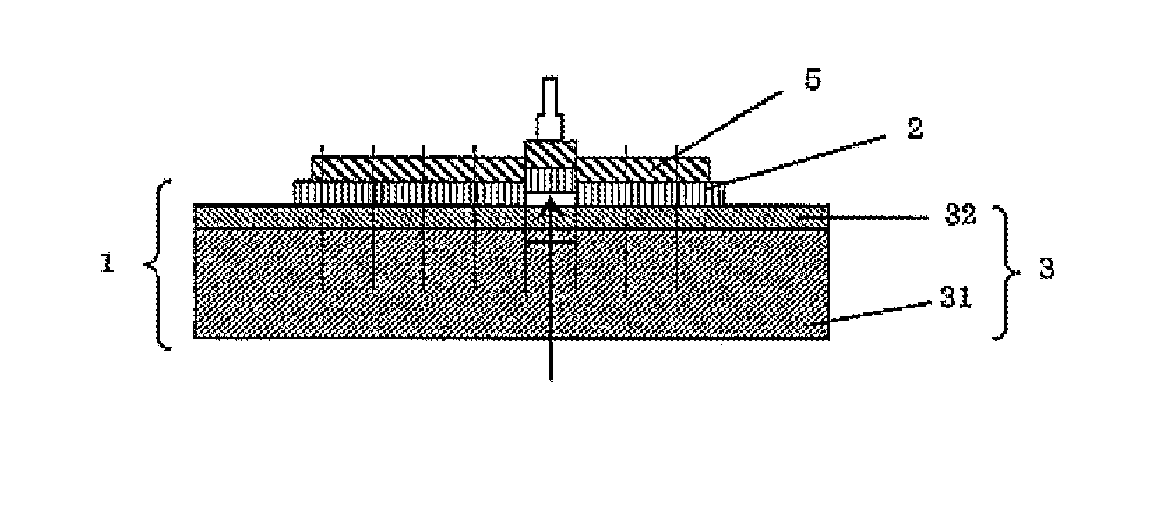
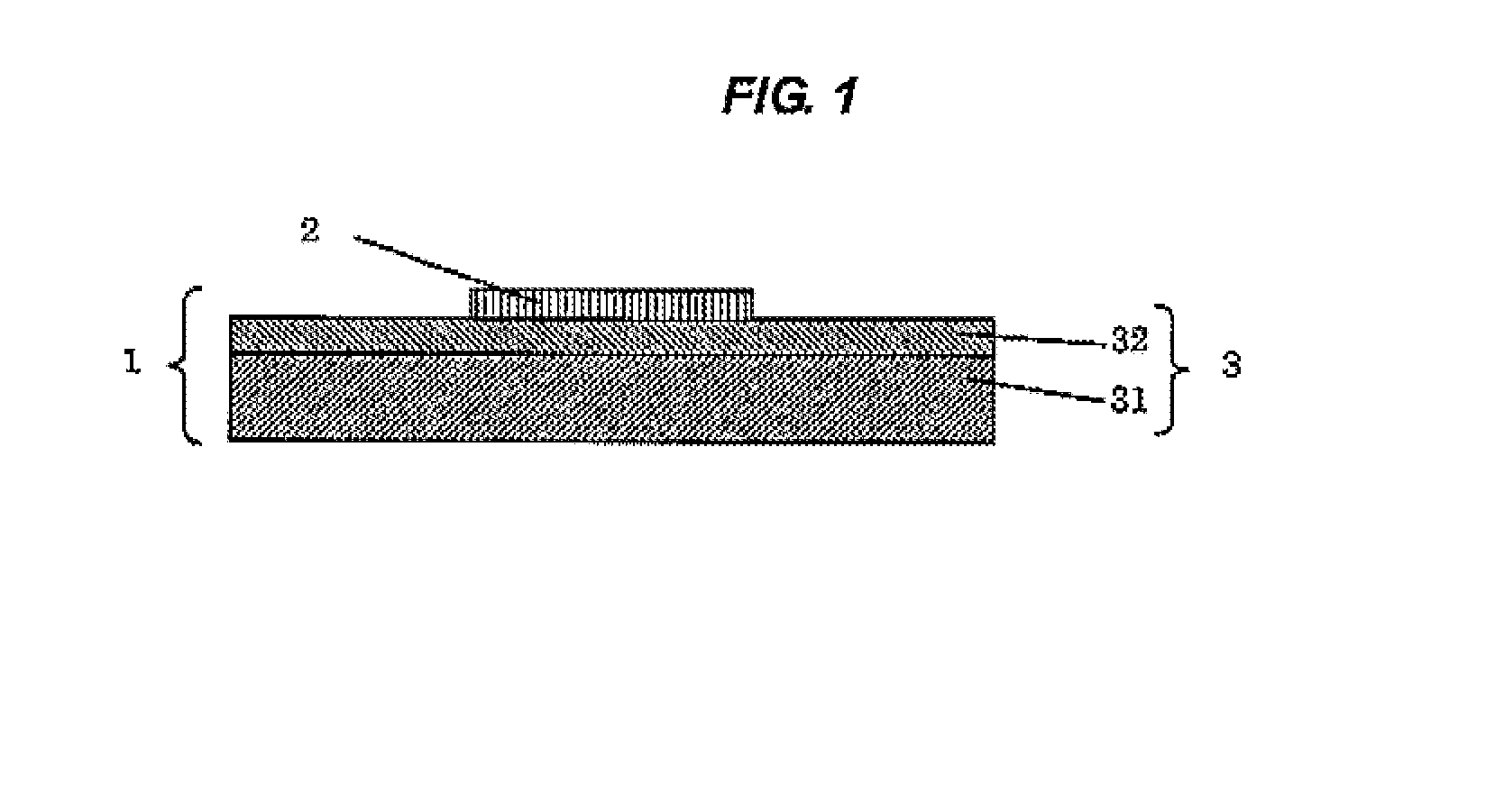
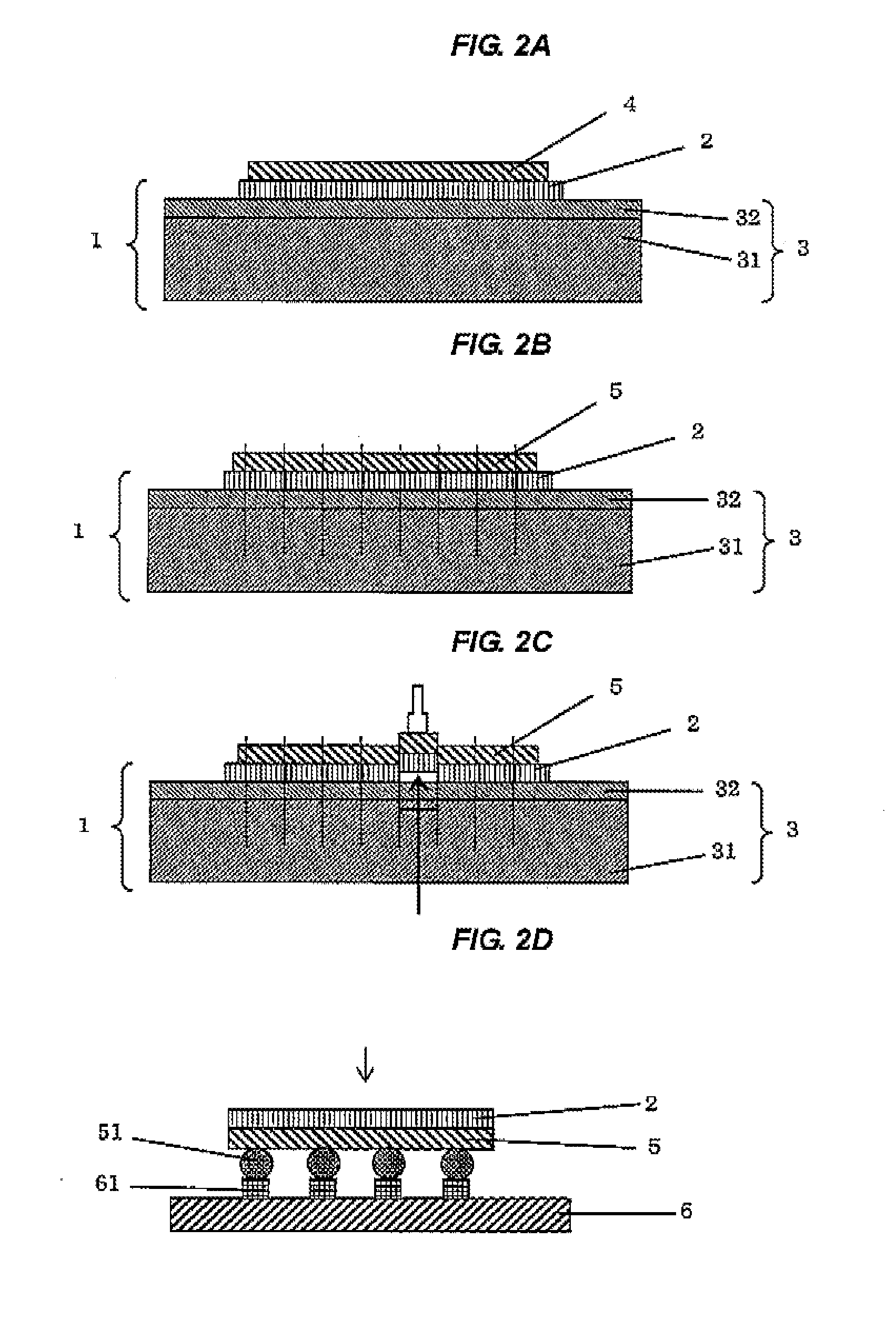
Dicing tape-integrated film for semiconductor back surface
a technology of tape-integrated film and back surface, which is applied in the direction of layered products, transportation and packaging, chemical instruments and processes, etc., can solve the problems of increasing the number of steps, increasing the cost and the like, and the damage of semiconductor chips, and achieve excellent laser marking properties and excellent holding for
- Summary
- Abstract
- Description
- Claims
- Application Information
AI Technical Summary
Benefits of technology
Problems solved by technology
Method used
Image

Examples
example 1
Manufacture of Film for Semiconductor Back Surface
[0166]113 parts of an epoxy resin (a trade name “EPICOAT 1004” manufactured by JER Co., Ltd.), 121 parts of a phenol resin (a trade name “MILEX XLC-4L” manufactured by Mitsui Chemicals, Inc.), 246 parts of sphere silica (a trade name “SO-25R” manufactured by Admatechs Co., Ltd., average particle diameter: 0.5 μm), and 3 parts of a black pigment (a trade name “Mitsubishi Carbon Black #47” manufactured by Mitsubishi Chemical Corporation) based on 100 parts of an acrylic acid ester-based polymer (a trade name “PARACRON W-197CM” manufactured by Negami Chemical Industrial Co., Ltd.) having ethyl acrylate and methyl methacrylate as main components were dissolved into methyl ethyl ketone to adjust a solid concentration to 23.6% by weight and a dispersed solution of the resin composition was prepared by means of a ball mill.
[0167]The resin composition solution was applied onto a releasably treated film as a release liner (separator) composed...
PUM
| Property | Measurement | Unit |
|---|---|---|
| particle diameter | aaaaa | aaaaa |
| thickness | aaaaa | aaaaa |
| thickness | aaaaa | aaaaa |
Abstract
Description
Claims
Application Information