[0014]The present invention has been devised in consideration of the foregoing problem and an object thereof is to provide a dicing tape-integrated film for semiconductor back surface capable of being utilized from the dicing step of the semiconductor
wafer to the flip chip bonding step of the semiconductor chip. Moreover, another object of the invention is to provide a dicing tape-integrated film for semiconductor back surface capable of exhibiting an excellent holding force in the dicing step of the semiconductor
wafer and further capable of exhibiting an excellent
laser marking property after the flip chip bonding step of the semiconductor chip.
[0015]As a result of intensive investigations for solving the above-mentioned conventional problems, the present inventors have found that, when a film for flip chip type semiconductor back surface is laminated on a pressure-sensitive
adhesive layer of a dicing tape having a base material and the pressure-sensitive adhesive layer to form the dicing tape and the film for flip chip type semiconductor back surface in an integrated fashion and the film for flip chip type semiconductor back surface contains a black
pigment, the laminate (dicing tape-integrated film for semiconductor back surface) where the dicing tape and the film for flip chip type semiconductor back surface are formed in an integrated fashion can be utilized from the dicing step of the semiconductor wafer to the flip chip bonding step of the semiconductor chip as well as an excellent holding force can be exhibited in the dicing step of the semiconductor wafer and further an excellent
laser marking property can be exhibited after the flip chip bonding step of the semiconductor chip, thereby accomplishing the invention.
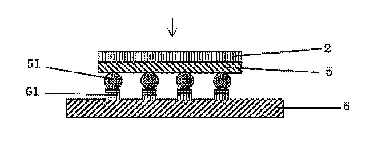
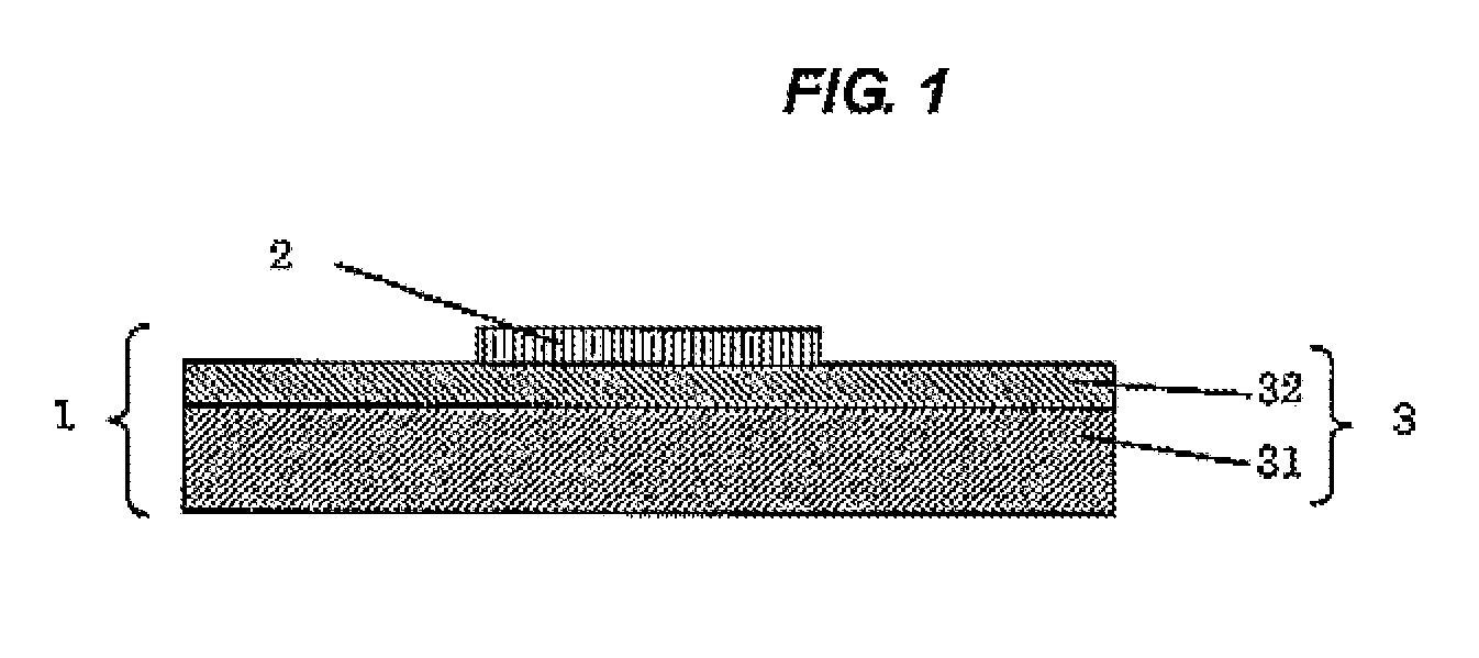
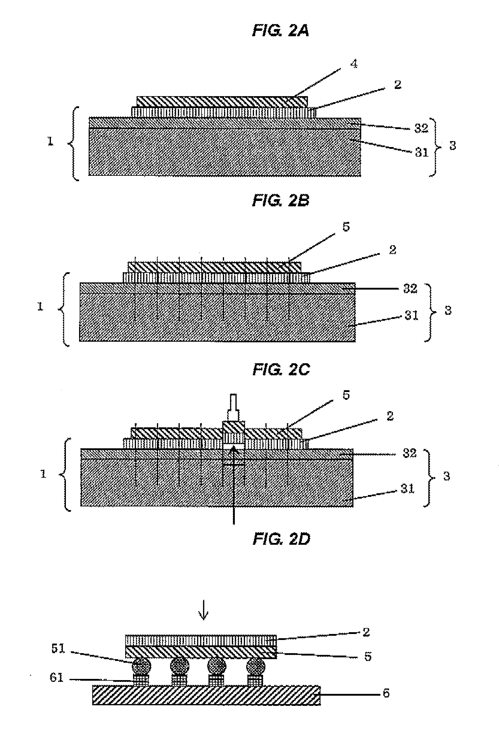
[0020]As above, the dicing tape-integrated film for semiconductor back surface according to the invention is formed in a form where the film for flip chip type semiconductor back surface is integrated with the dicing tape having the base material and the pressure-sensitive adhesive layer, and a black
pigment is used as a coloring agent in the film for flip chip type semiconductor back surface. Therefore, by attaching the dicing tape-integrated film for semiconductor back surface onto a workpiece (semiconductor wafer) at dicing a wafer (semiconductor wafer), the workpiece can be effectively diced while being held. Also, after the workpiece is diced to form a chip-shaped workpiece (semiconductor chip), the chip-shaped workpiece can be easily peeled from the pressure-sensitive adhesive layer of the dicing tape with an excellent picking-up property together with the film for flip chip type semiconductor back surface, and the back surface-protected chip-shaped workpiece can be easily obtained. In addition, since a film for flip chip type semiconductor back surface in which a black pigment is used as a coloring agent is formed on the back surface of the chip-shaped workpiece, the chip-shaped workpiece has an excellent
laser marking property. Needless to say, the chip-shaped workpiece has an excellent appearance property since a film for flip chip type semiconductor back surface in which a black pigment is used as a coloring agent is attached to the back surface with an excellent close adhesiveness.
[0021]Furthermore, in the dicing tape-integrated film for semiconductor back surface of the invention, since the dicing tape and the film for flip chip type semiconductor back surface are formed in an integrated fashion as mentioned above, the film for flip chip type semiconductor back surface can also be attached at the time when the dicing tape is attached to the back surface of the semiconductor wafer before the dicing step and thus a step of attaching the film for flip chip type semiconductor back surface alone (film for flip chip type semiconductor back surface-attaching step) is not necessary. In addition, in the subsequent dicing step and picking-up step, since the film for flip chip type semiconductor back surface is attached on the back surface of the semiconductor wafer or the back surface of the semiconductor chip formed by dicing, the semiconductor wafer or the semiconductor chip can be effectively protected and thus the damage of the semiconductor chip can be suppressed or prevented in the dicing step or subsequent steps (picking-up step, etc.).
[0029]Since a dicing tape and a wafer back surface protective film are formed in an integrated fashion as well as the film for flip chip type semiconductor back surface contains a black pigment, the dicing tape-integrated film for semiconductor back surface according to the invention can be utilized from the dicing step of the semiconductor wafer to the flip chip bonding step of the semiconductor chip. Specifically, the dicing tape-integrated film for semiconductor back surface according to the invention can exhibit an excellent holding force in the dicing step of the semiconductor wafer and further can exhibit an excellent laser marking property during and after the flip chip bonding step of the semiconductor chip. Moreover, in the flip chip bonding step and the like, since the back surface of the semiconductor chip is protected with the film for flip chip type semiconductor back surface, breakage, chipping, warp, and the like of the semiconductor chip can be effectively suppressed or prevented. Needless to say, the dicing tape-integrated film for semiconductor back surface according to the invention can effectively exhibit functions thereof in steps other than the steps from the dicing step to the flip chip bonding step of the semiconductor chip.

