
Sampling circuit for ADC

a sampling circuit and adc technology, applied in the field of sampling circuits, can solve the problems of serious effect on the accuracy of differential sampling output signals, inability to eliminate and non-linear errors, so as to reduce the harmonic distortion of sampling circuits, improve the linearity of sampling fet, and reduce the impact of clock feedthrough

Inactive Publication Date: 2014-06-26
IPGOAL MICROELECTRONICS (SICHUAN) CO LTD
View PDF4 Cites 27 Cited by
  • Summary
  • Abstract
  • Description
  • Claims
  • Application Information

AI Technical Summary

Benefits of technology

The present invention provides a sampling circuit for ADC that improves the linearity of sampling FET, reduces harmonic distortion, and improves sampling speed and accuracy by decreasing the impact of clock feedthrough on signal sampling. The circuit samples external input signals using an auxiliary circuit and outputs the signals after sampling to a clock feedthrough circuit. The clock feedthrough circuit processes the signals to generate a transient compensation voltage that can effectively eliminate the impacts of clock feedthrough in the sampling circuit. This results in improved signal-to-noise ratios and reduced distortion in the sampled signals.

Problems solved by technology

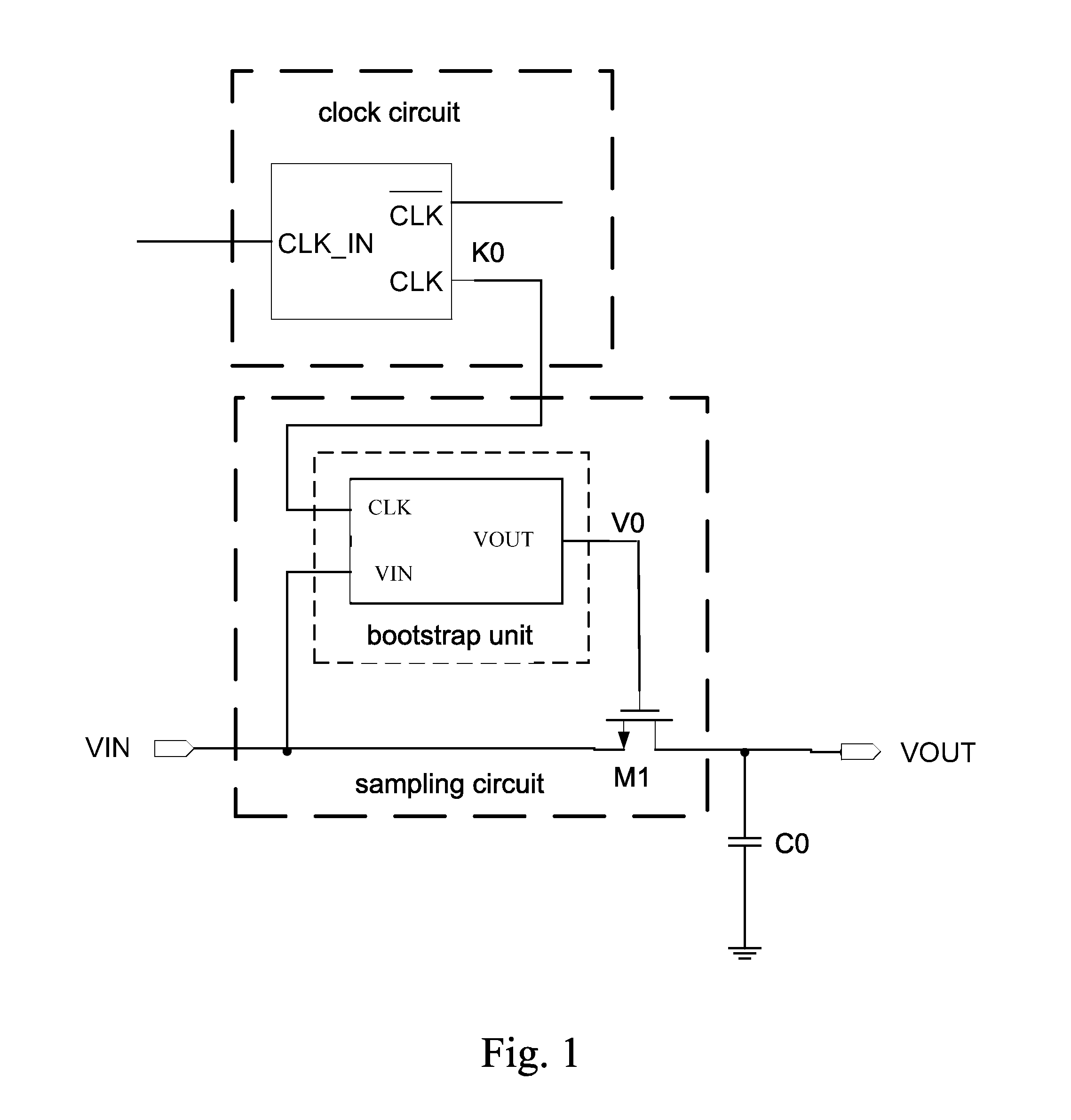
However, while adopting the sampling circuit having the bootstrap structure, error introduced by the clock feedthrough is related to the signals inputted, and thus non-linear error is introduced, and the impact of the clock feedthrough is not capable of being eliminated by adopting a fully-differential structure amplifier.
In addition, the greater the parasitic capacitance of the EFT M1, the greater the amplitude of the input signal, and the more obvious of the nonlinearity introduced by the clock feedthrough effect, which has a serious effect on the accuracy of the differential sampling output signal.

Method used


Image

  • Sampling circuit for ADC
  • Sampling circuit for ADC
  • Sampling circuit for ADC

Examples


Embodiment Construction

[0043]Combining with the accompanying drawings, preferred embodiment of the present invention is illustrated as follows. As mentioned above, the present invention provides a sampling circuit for ADC, which improves linearity of sampling FET, reduces harmonic distortion of the sampling circuit and improves sampling speed thereof, and improves sampling accuracy of the sampling circuit for ADC.

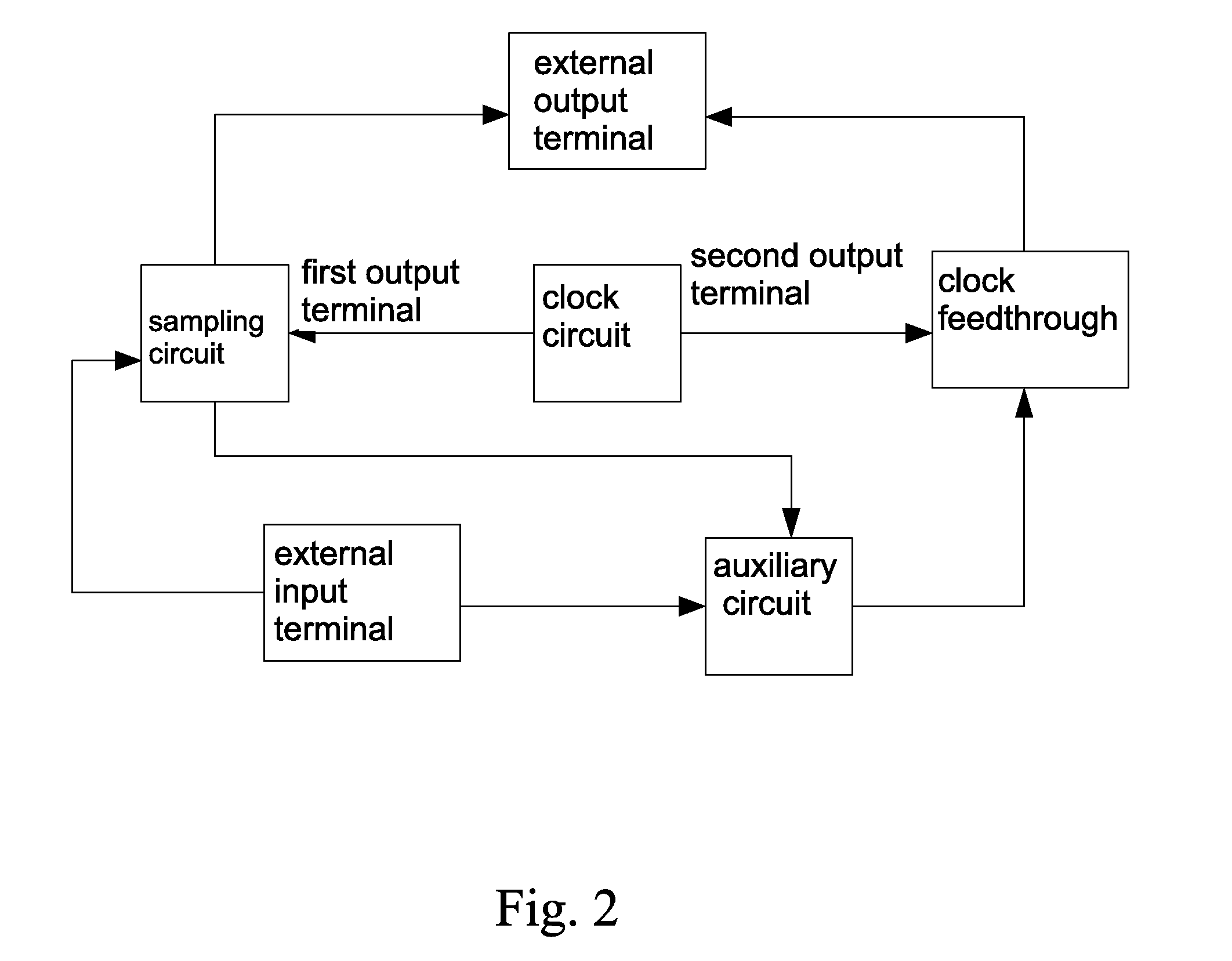
[0044]Referring to FIG. 2 of the drawings, according to a preferred embodiment of the present invention is illustrated, a sampling circuit for ADC comprising:

[0045]an external input terminal,

[0046]a sampling circuit and an auxiliary circuit which are connected with the external input terminal,

[0047]a clock circuit and an external output terminal which are connected with the sampling circuit, and

[0048]a clock feedthrough circuit connected with the auxiliary circuit, wherein the clock feedthrough circuit is respectively connected with the clock circuit and the external output terminal,

[0049]wherein...


PUM


Abstract

A sampling circuit for ADC includes an external input terminal, a sampling circuit and an auxiliary circuit which are connected with the external input terminal, a clock circuit and an external output terminal which are connected with the sampling circuit, and a clock feedthrough circuit connected with the auxiliary circuit, wherein the clock feedthrough circuit is respectively connected with the clock circuit and the external output terminal. The sampling circuit for ADC of the present invention decreases the impact of clock feedthrough on signal sampling, improves linearity of sampling FET, reduces harmonic distortion of the sampling circuit and improves sampling speed thereof, and improves sampling accuracy of the sampling circuit for ADC.

Description

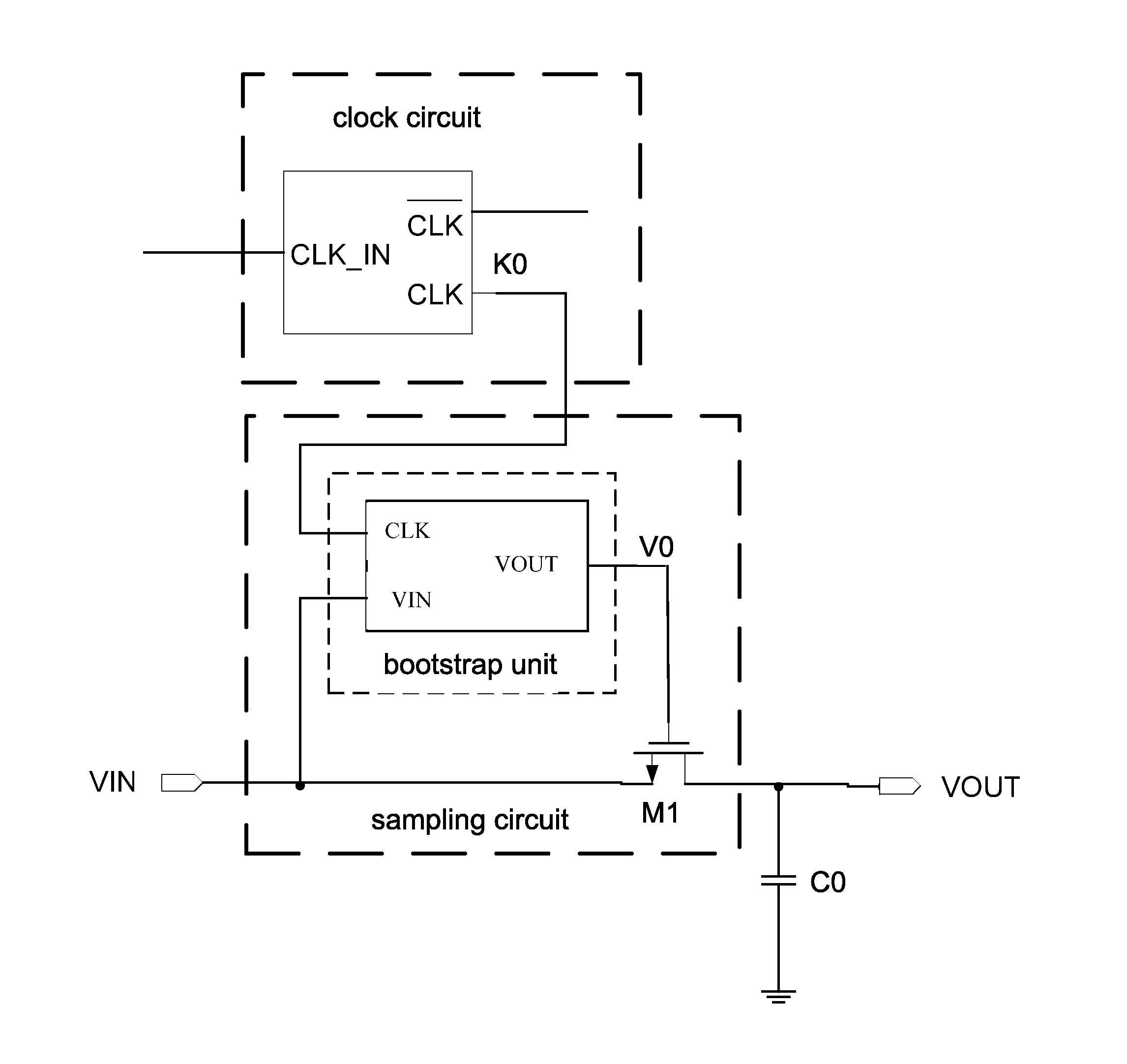
BACKGROUND OF THE PRESENT INVENTION [0001]1. Field of Invention[0002]The present invention relates to a field of a sampling circuit, and more particularly to a sample-and-hold circuit for ADC (Analog-to-Digital Converter).[0003]2. Description of Related Arts[0004]In the circuit for ADC (Analog-to-Digital Converter), in order to ensure the accuracy and speed of the ADC, the input sampling terminal have to employ a bootstrap structure to ensure the linearity of the input sampling switch and to expand the range of the input signal as well. However, while adopting the sampling circuit having the bootstrap structure, error introduced by the clock feedthrough is related to the signals inputted, and thus non-linear error is introduced, and the impact of the clock feedthrough is not capable of being eliminated by adopting a fully-differential structure amplifier.[0005]Referring to FIG. 1 of the drawings, the conventional sampling circuit for ADC comprises a clock circuit, a sampling circuit...

Claims


Application Information

Patent Timeline
IPC IPC(8): H03M1/12
CPCH03M1/124G11C27/024
Inventor YANG, BAODING
Owner IPGOAL MICROELECTRONICS (SICHUAN) CO LTD
Learn More