

Printed substrate design system, and printed substrate design method
- Summary
- Abstract
- Description
- Claims
- Application Information
AI Technical Summary
Benefits of technology
Problems solved by technology
Method used
Image

Examples
Embodiment Construction
[0083]Hereunder, the present invention is described through exemplary embodiments of the invention, however the exemplary embodiments below do not limit the invention according to the claims. Moreover, all combinations of characteristics described in the exemplary embodiments are not always required for the problem solving means of the invention.
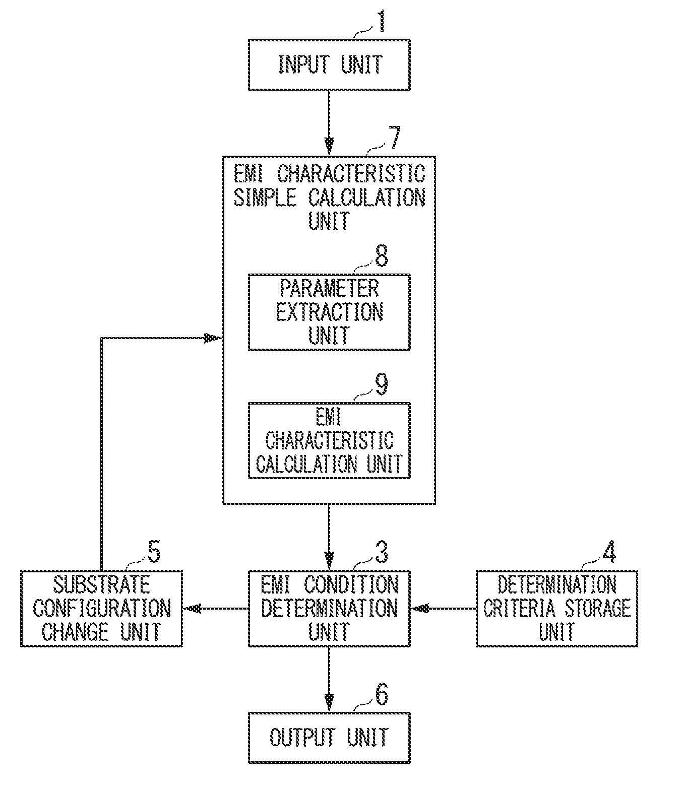
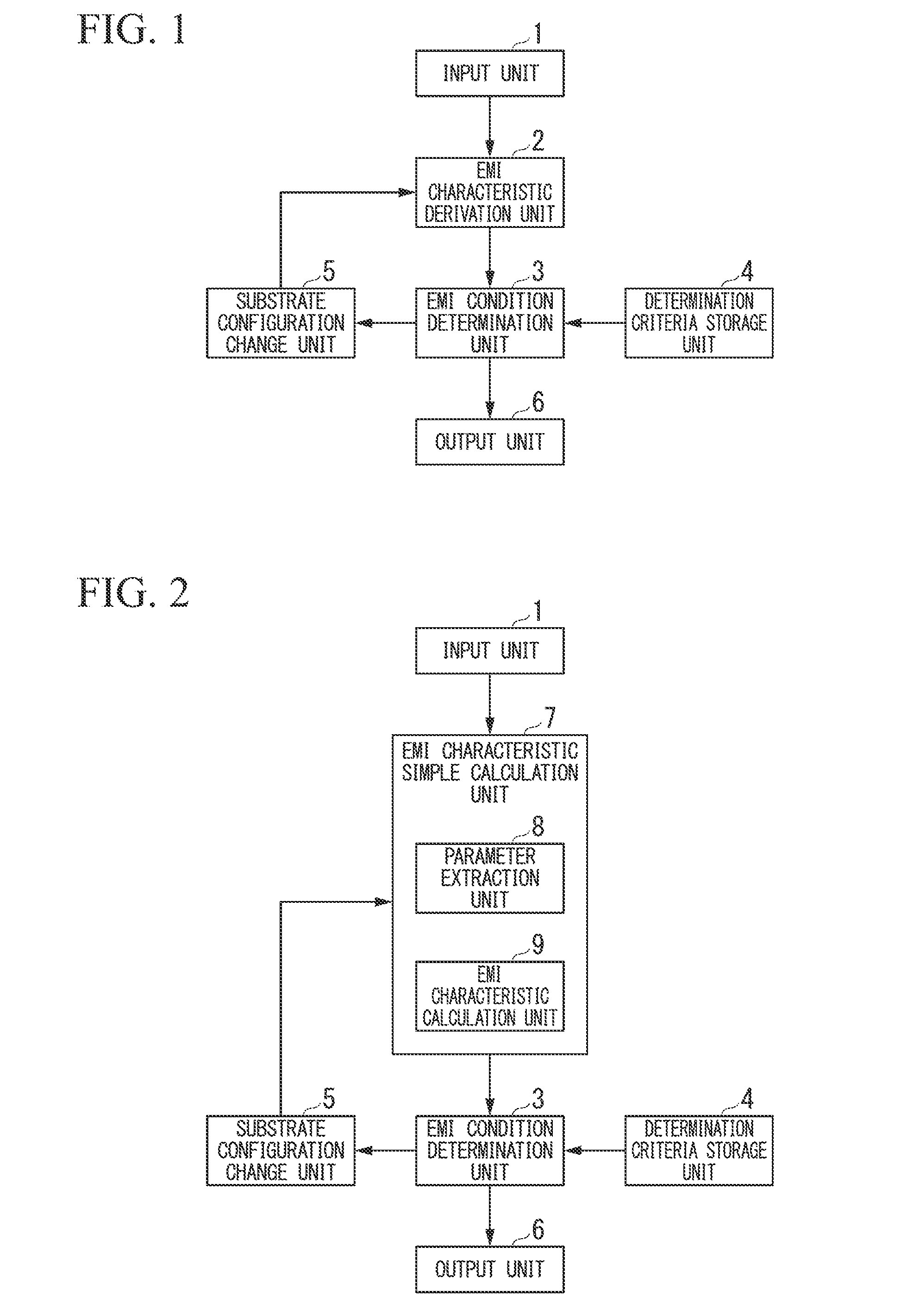
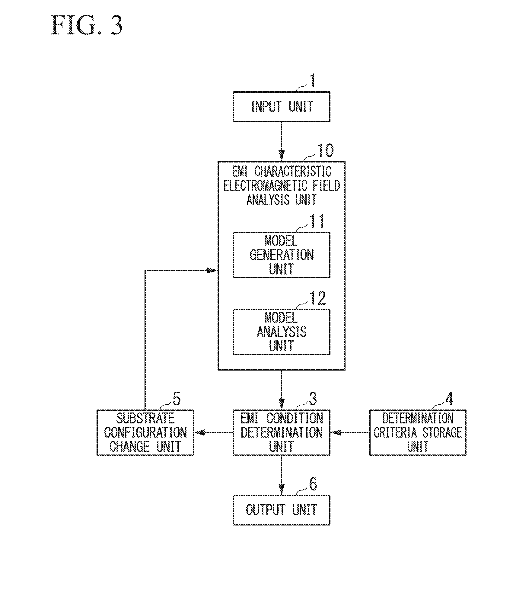
[0084]FIG. 1 shows an example of a block configuration of a printed substrate design system according to a first exemplary embodiment of the present invention. The printed substrate design system is a system that designs a substrate configuration of a printed substrate on which ICs and other passive components are to be mounted and to which a cable is to be connected.
[0085]The printed substrate design system of the first exemplary embodiment includes an input unit 1, an EMI characteristic derivation unit 2, an EMI condition determination unit 3, a determination criteria storage unit 4, a substrate configuration change unit 5, and an output u...
PUM
 Abstract
Description
Claims
Application Information