Field effect transistor with channel core modified for a backgate bias and method of fabrication

a field effect transistor and backgate bias technology, applied in the field of nanowire field effect transistors, can solve the problems of difficult to achieve multiple vt's for nwfets and finfets without increasing transistor variability

Active Publication Date: 2014-07-03
RENESAS ELECTRONICS CORP
View PDF5 Cites 25 Cited by
  • Summary
  • Abstract
  • Description
  • Claims
  • Application Information

AI Technical Summary

Benefits of technology

[0011]In view of the foregoing and other exemplary problems, drawbacks, and disadvantages of the conventional methods and systems, an exemplary feature of the present invention is to provide a structure and method of fabric

Problems solved by technology

However, particularly with the miniaturization of electronic devices, as exemplified by the use of NWFETs and finFETs and using conven

Method used


Image

  • Field effect transistor with channel core modified for a backgate bias and method of fabrication
  • Field effect transistor with channel core modified for a backgate bias and method of fabrication
  • Field effect transistor with channel core modified for a backgate bias and method of fabrication

Examples


Embodiment Construction

[0032]Referring now to the drawings, and more particularly to FIGS. 4-14D, exemplary embodiments of the method and structures of the present invention will now be explained.

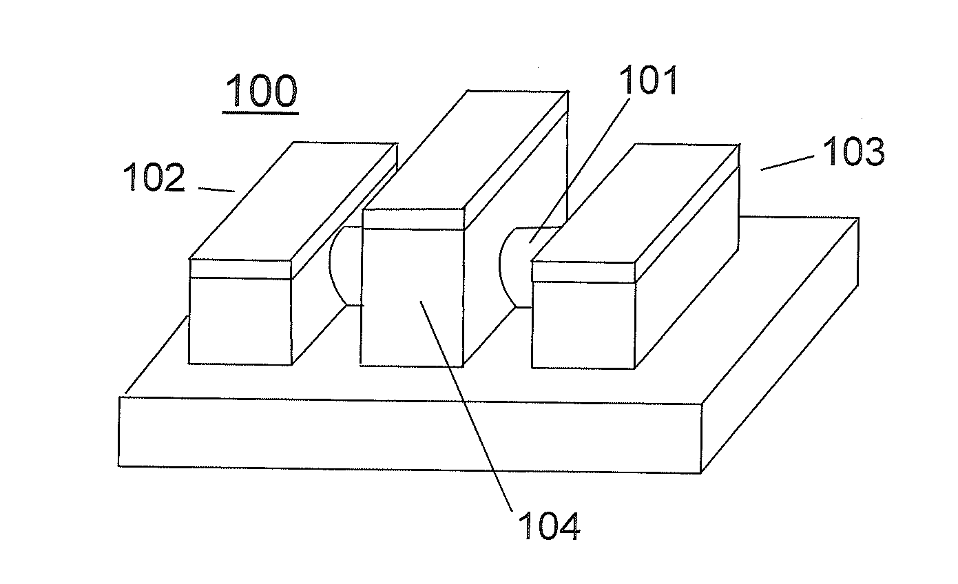
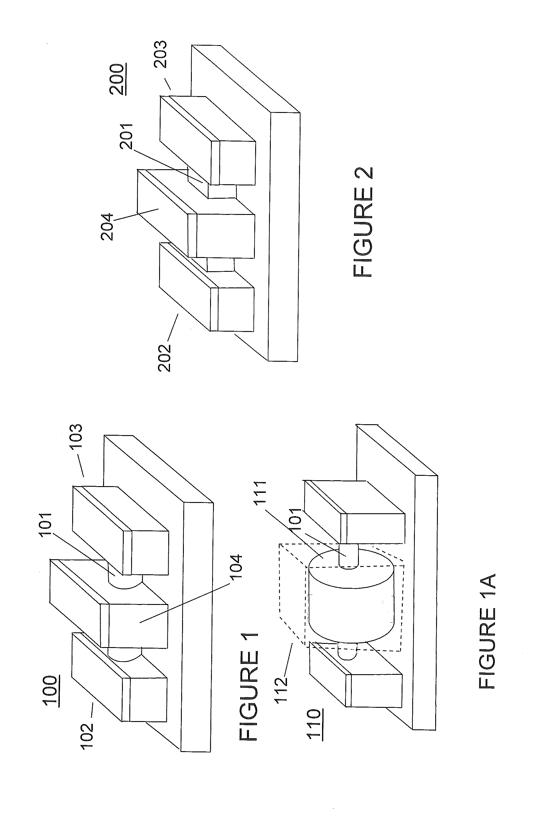
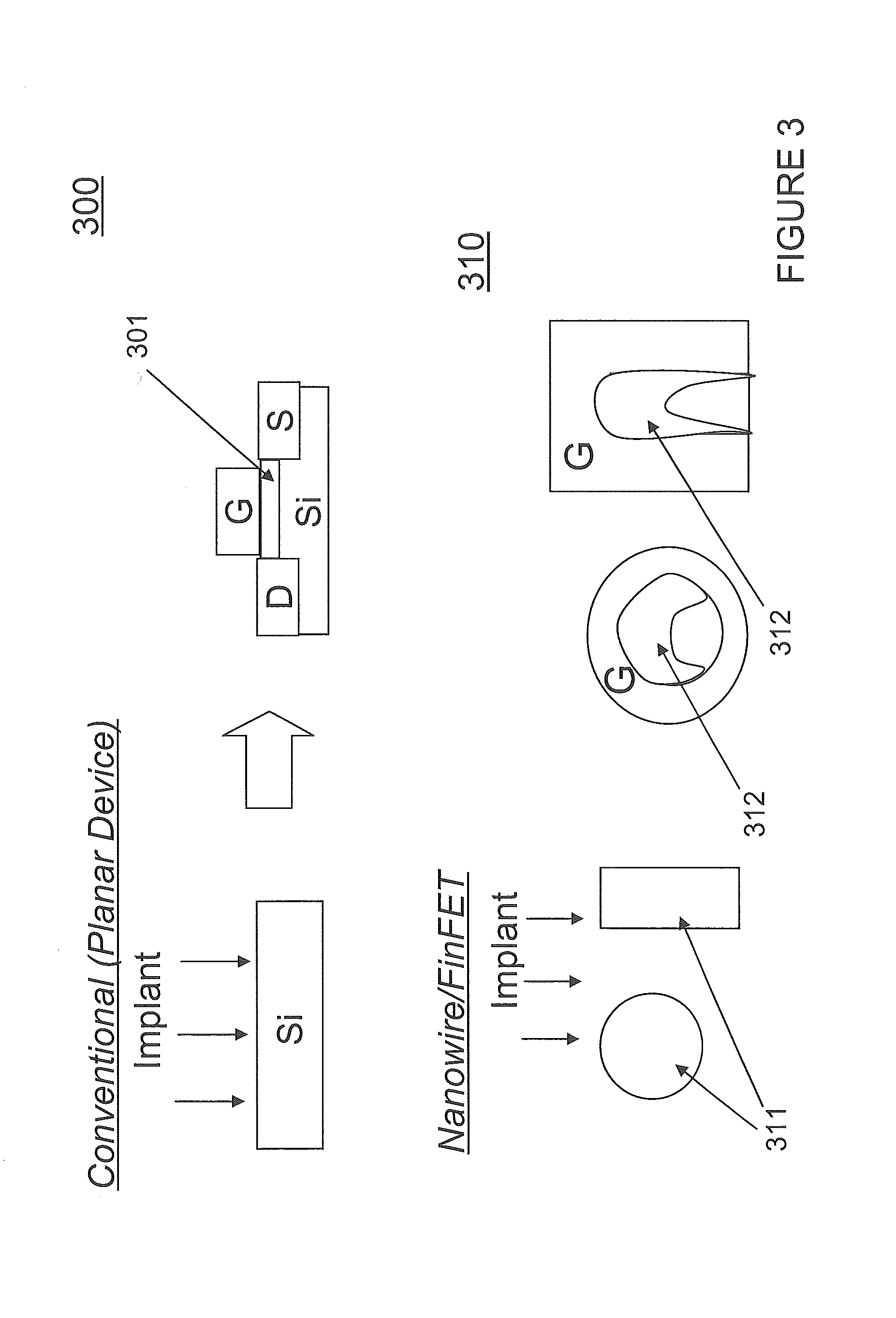
[0033]To begin, FIG. 4 exemplarily illustrates a cross-sectional view 400 of a nanowire channel 401 of an NWFET or fin 402 of a finFET of the present invention, as modified to incorporate an electrode material, such as polysilicon, as used herein to explain an exemplary embodiment of the present invention, as a core 403 of a channel 404, surrounded by a gate dielectric layer 405, which, in turn, is surrounded by the gate structure including, for example, a layer of metal 406 and / or a layer of doped polysilicon. As typical with conventional nanowire channel devices, the channel 404 would typically be comprised of Si, SiGe, or Si / SiGe.

[0034]However, instead of polysilicon, other materials such as the metal tungsten (W) can also be used for the backbias electrode, as long as it at can be inserted into a nanowire in ...


PUM


Abstract

A semiconductor device includes a substrate and a source structure and a drain structure formed on the substrate. At least one nanowire structure interconnects the source structure and drain structure and serves as a channel therebetween. A gate structure is formed over said at least one nanowire structure to provide a control of a conductivity of carriers in the channel, and the nanowire structure includes a center core serving as a backbias electrode for the channel.

Description

[0001]This Application is a Non-Provisional Application of Provisional Application No. 61 / 746,991, filed on Dec. 28, 2012, and claims priority thereto.BACKGROUND OF THE INVENTION[0002]1. Field of the Invention[0003]The present invention relates generally to a NanoWire Field Effect Transistor (NWFET) or a finFET in which a channel core is modified to incorporate a feature for controlling threshold voltage. More specifically, the core of the nanowire channel of the NWFET or the core of the fin of the finFET is filled with an electrode material to which can be applied a backbias voltage.[0004]2. Description of the Related Art[0005]A recent trend in integrated circuit (IC) design is the use of nanowire transistors. FIG. 1 shows exemplarily a conventional nanowire field effect transistor (NWFET) configuration 100, wherein the nanowire 101 serves as the channel interconnecting the source 102 and drain 103. The gate 104 serves to control conductivity of the channel nanowire 101.[0006]As sh...

Claims


Application Information

Patent Timeline
IPC IPC(8): H01L29/775H01L29/66H01L29/78
CPCH01L29/775H01L29/785H01L29/66795H01L29/66439H01L29/0673B82Y10/00H01L21/283H01L21/30604H01L29/0611H01L29/1087H01L29/16H01L29/161H01L29/42392H01L29/45H01L29/66742H01L29/778H01L29/78648H01L29/78696
Inventor HIRAI, TOMOHIRONAGUMO, TOSHIHARU
Owner RENESAS ELECTRONICS CORP
Why Eureka
Try Eureka