Stacked multi-chip package and method of making same

a multi-chip package and integrated circuit technology, applied in the direction of semiconductor devices, electrical equipment, semiconductor/solid-state device details, etc., can solve the problems of delay, loss, noise in signals,

Inactive Publication Date: 2014-07-03
IBM CORP
View PDF0 Cites 15 Cited by
  • Summary
  • Abstract
  • Description
  • Claims
  • Application Information

AI Technical Summary

Problems solved by technology

However, a problem with current stacked integrated circuit chip packages is signals from the first integrated circuit chips have to travel through all the second integrated circuit chips to get to the package substrate causing delay, loss, and noise in the signals.

Method used


Image

  • Stacked multi-chip package and method of making same
  • Stacked multi-chip package and method of making same
  • Stacked multi-chip package and method of making same

Examples


Embodiment Construction

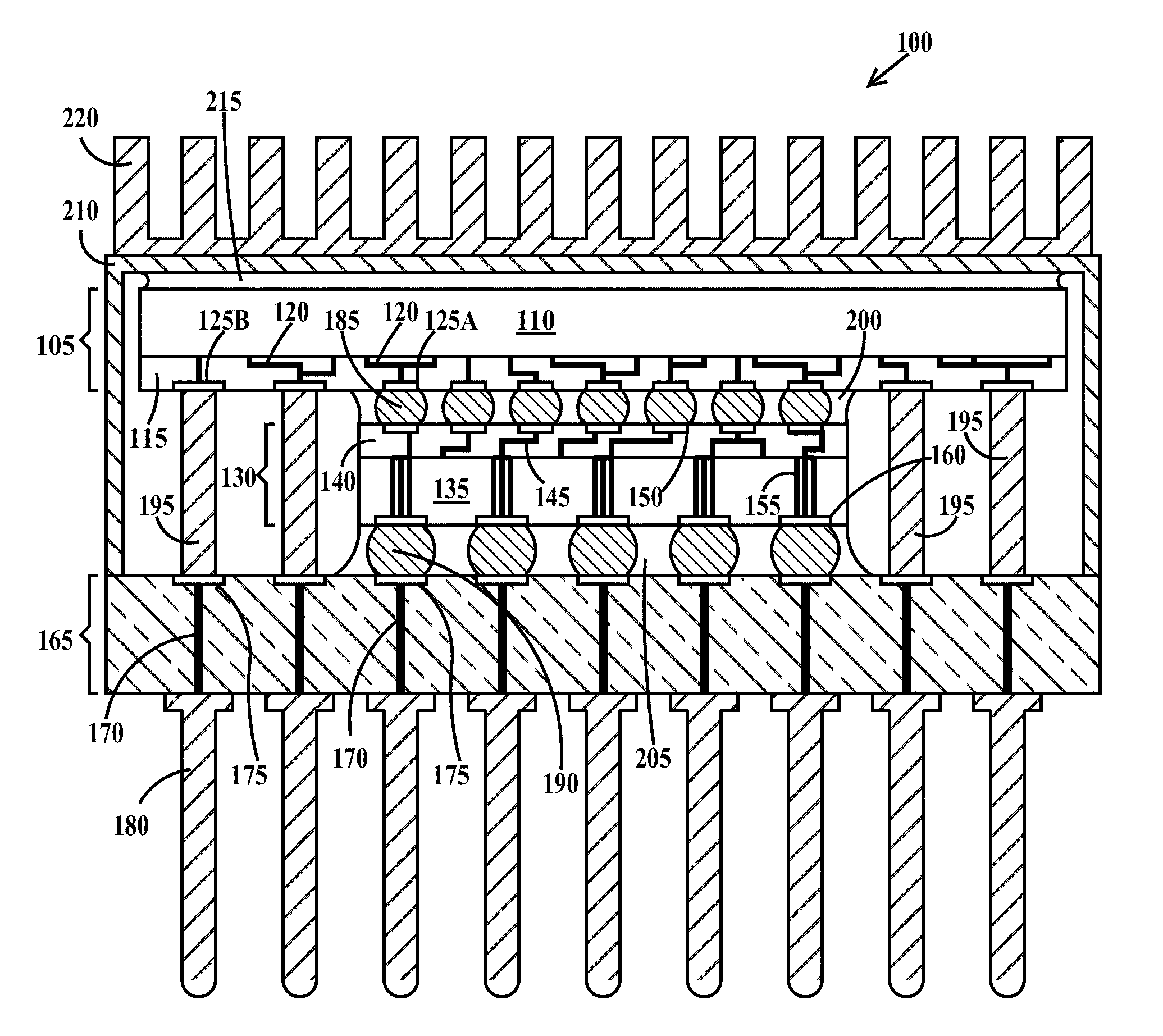
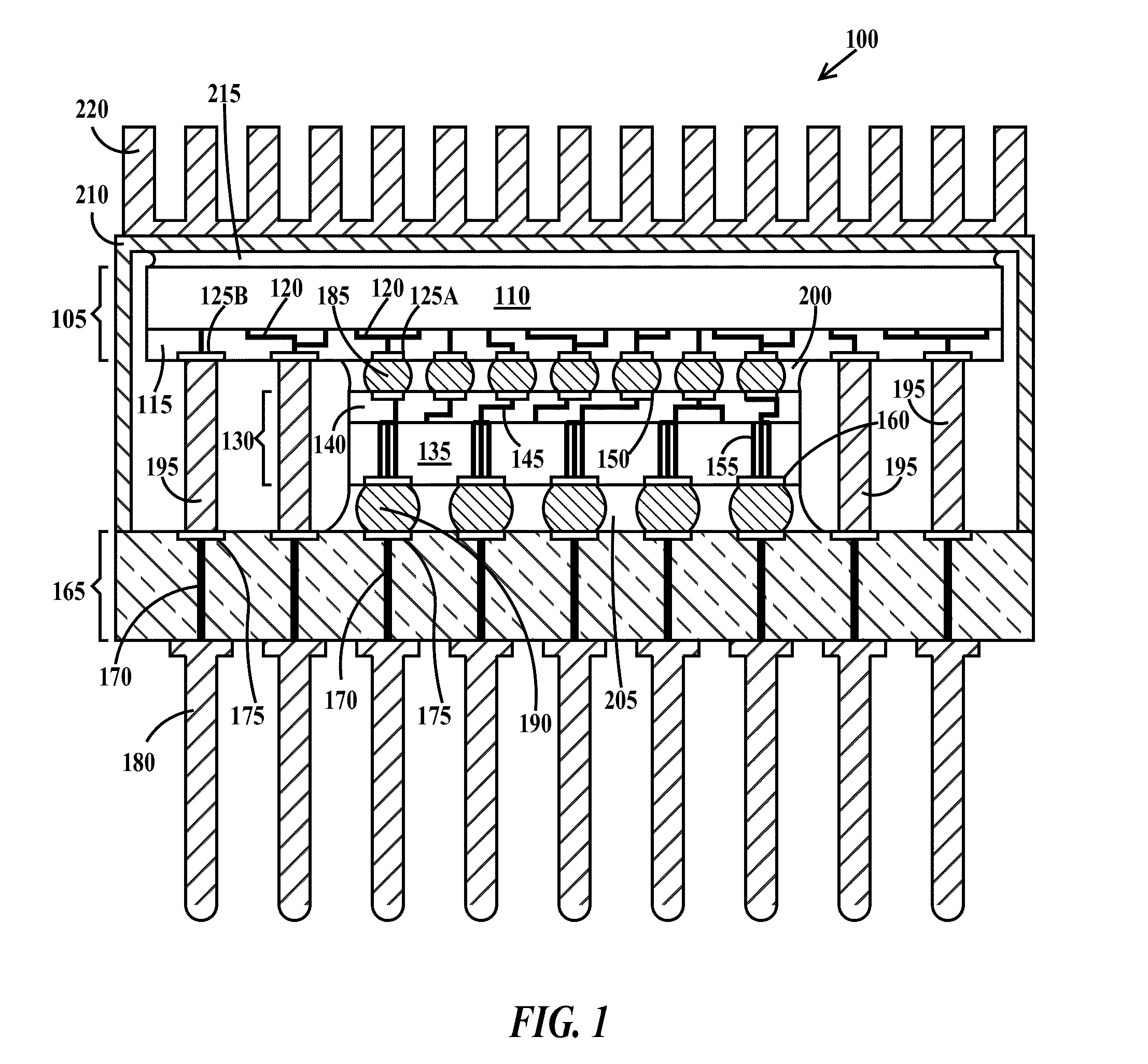
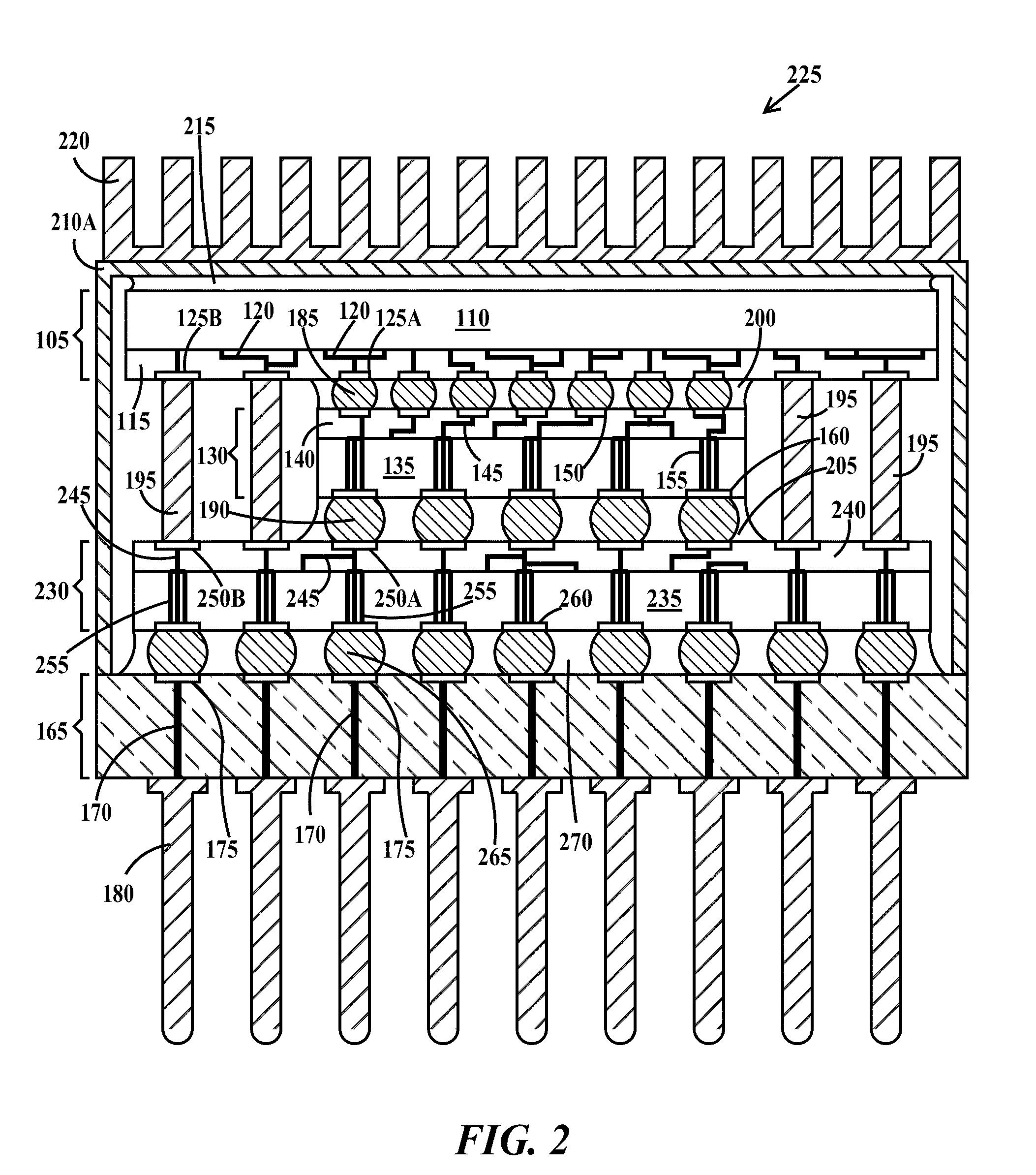
[0013]The embodiments of the present invention provide for a stacked integrated circuit chip package (hereinafter “stacked chip package” that sends a first group of signals from an first integrated circuit chip to a package substrate through an intervening integrated circuit chip having through wafer vias and sends a second group of signals from the first integrated circuit chip to the package substrate directly or indirectly through electrically conductive columns external to the integrated circuit chips.

[0014]An integrated circuit chip is an electronic circuit manufactured by lithography, etching and the patterned diffusion of trace elements into the surface of a thin substrate of semiconductor material to form active and passive devices. Integrated circuits contain transistors (e.g., NFETs and PFETs), resistors and capacitors. Additional integrated circuits contain patterned electrically conductive interconnections (e.g., wires) that connect the devices into functional circuits. ...


PUM


Abstract

Stacked multichip packages and methods of making multichip packages. A method includes using a boat having different depth openings corresponding to the length of column interconnections of the completed multichip package and masks to place proper length columns in the corresponding depth openings; placing an integrated circuit chip on the boat and attaching exposed upper ends of the columns to respective chip pads of the integrated circuit using a first solder reflow process and attaching a preformed package substrate integrated circuit chip stack to the integrated circuit and attached columns using a second solder reflow process.

Description

TECHNICAL FIELD[0001]The present invention relates to the field of integrated circuit chip packages; more specifically, it relates to stacked integrated circuit chip packages.BACKGROUND[0002]Integrated circuit chip stacking is a technology that allows for a high density form factor by stacking integrated circuit chips on top of each other. However, a problem with current stacked integrated circuit chip packages is signals from the first integrated circuit chips have to travel through all the second integrated circuit chips to get to the package substrate causing delay, loss, and noise in the signals. Accordingly, there exists a need in the art to eliminate the deficiencies and limitations described hereinabove.BRIEF SUMMARY[0003]A first aspect of the present invention is a method, comprising: providing a boat having first openings extending a first depth into the boat and second openings extending a second and different depth into the boat; placing a first mask on the boat, first th...

Claims


Application Information

Patent Timeline
Patent Type & Authority Applications(United States)
IPC IPC(8): H01L23/00
CPCH01L24/17H01L24/81H01L24/05H01L24/06H01L24/11H01L24/14H01L24/29H01L24/32H01L24/73H01L24/92H01L24/97H01L25/0657H01L25/50H01L2224/0401H01L2224/0557H01L2224/06181H01L2224/11003H01L2224/11005H01L2224/11334H01L2224/13111H01L2224/13147H01L2224/1403H01L2224/141H01L2224/16145H01L2224/16227H01L2224/17051H01L2224/17181H01L2224/2929H01L2224/29386H01L2224/32145H01L2224/32225H01L2224/73204H01L2224/73253H01L2224/81075H01L2224/81815H01L2224/92125H01L2224/97H01L2225/06513H01L2225/06517H01L2225/06541H01L2225/06555H01L2225/06589H01L2924/15311H01L2924/15312H01L2924/15787H01L2924/16235H01L2924/16251H01L2224/16225H01L2924/00H01L2924/01083H01L2924/01046H01L2924/01047H01L2224/81H01L2924/00014
Inventor AYOTTE, STEPHEN P.HILL, DAVID J.SULLIVAN, TIMOTHY M.
Owner IBM CORP
Why Eureka
Try Eureka