Systems and methods for semiconductor line scribe centering

Inactive Publication Date: 2014-07-03
GLOBALFOUNDRIES INC
View PDF12 Cites 1 Cited by
  • Summary
  • Abstract
  • Description
  • Claims
  • Application Information

AI Technical Summary

Benefits of technology

[0006]In a first aspect of the invention, a method comprises placing and measuring substantially identical test macros within a chip and in a scribe line. The method also comprises establishing an estimate correlation between scribe line measurements taken during a manufacturing process and product measurements taken on a final product. The method further comprises determining empirical scribe line specification limits consistent with established product screen limits. The method further comprises adjusting the manufacturing process in order to optimize performance to the empirical scribe line specification limits.
[0007]In another aspect of the invention, a method comprises: creating specification limits for a product and scribe line measurements; embedding monitor devices in testable on-product structures and testable scribe-line st

Problems solved by technology

Because one set of data are used for process control while another set are used to screen finished products; differences between the two can lead to false reje

Method used


Image

  • Systems and methods for semiconductor line scribe centering
  • Systems and methods for semiconductor line scribe centering
  • Systems and methods for semiconductor line scribe centering

Examples


Embodiment Construction

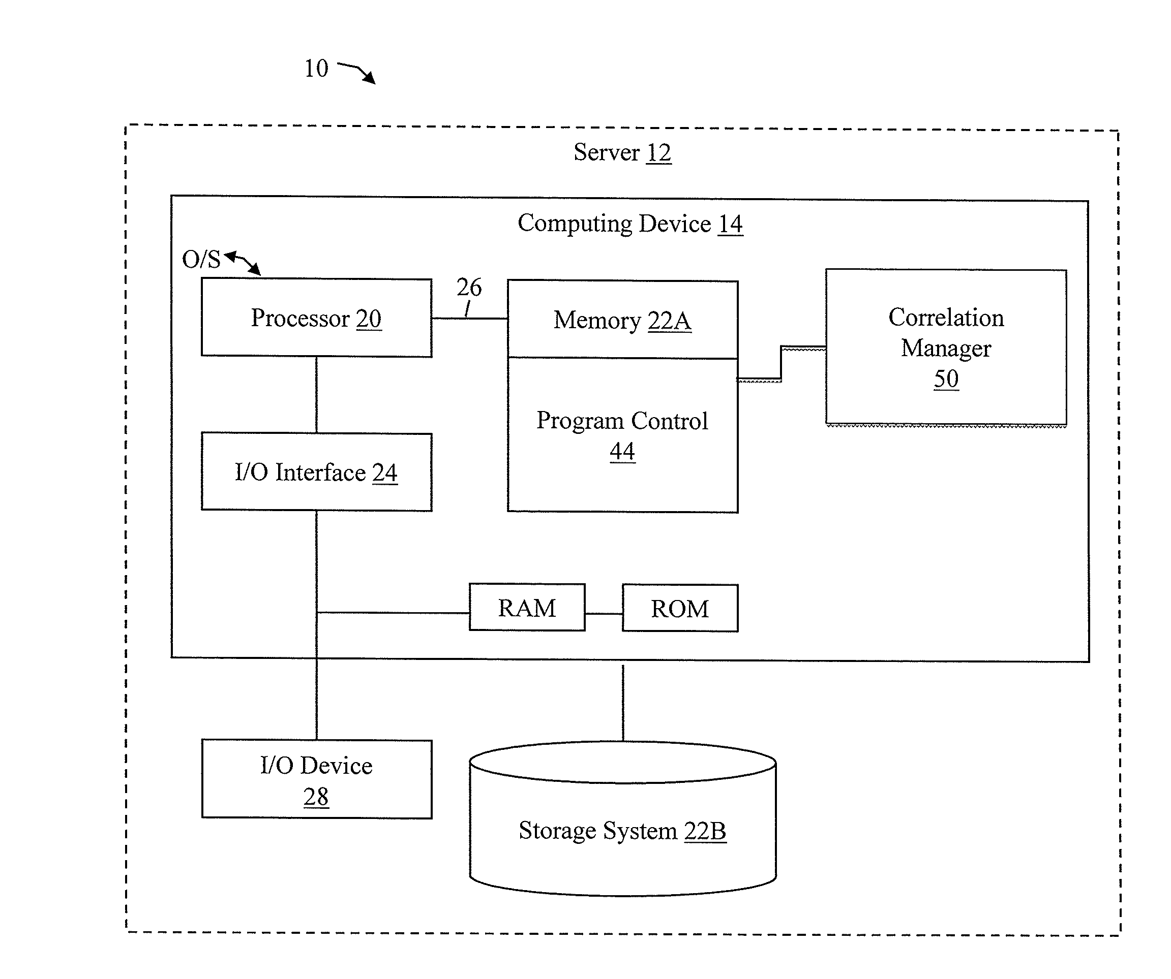
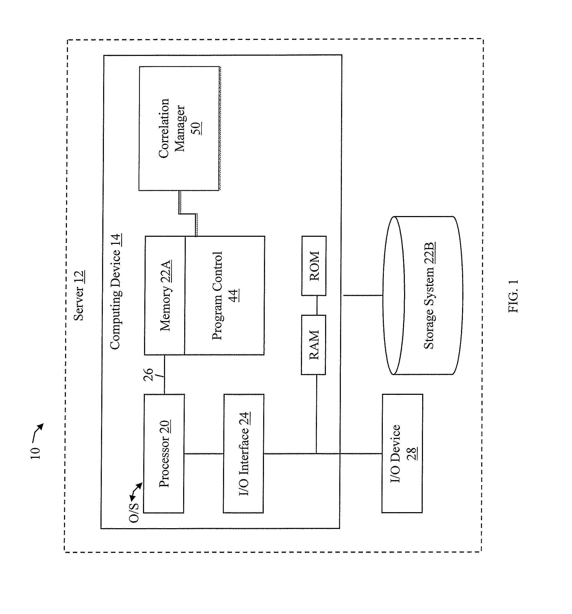
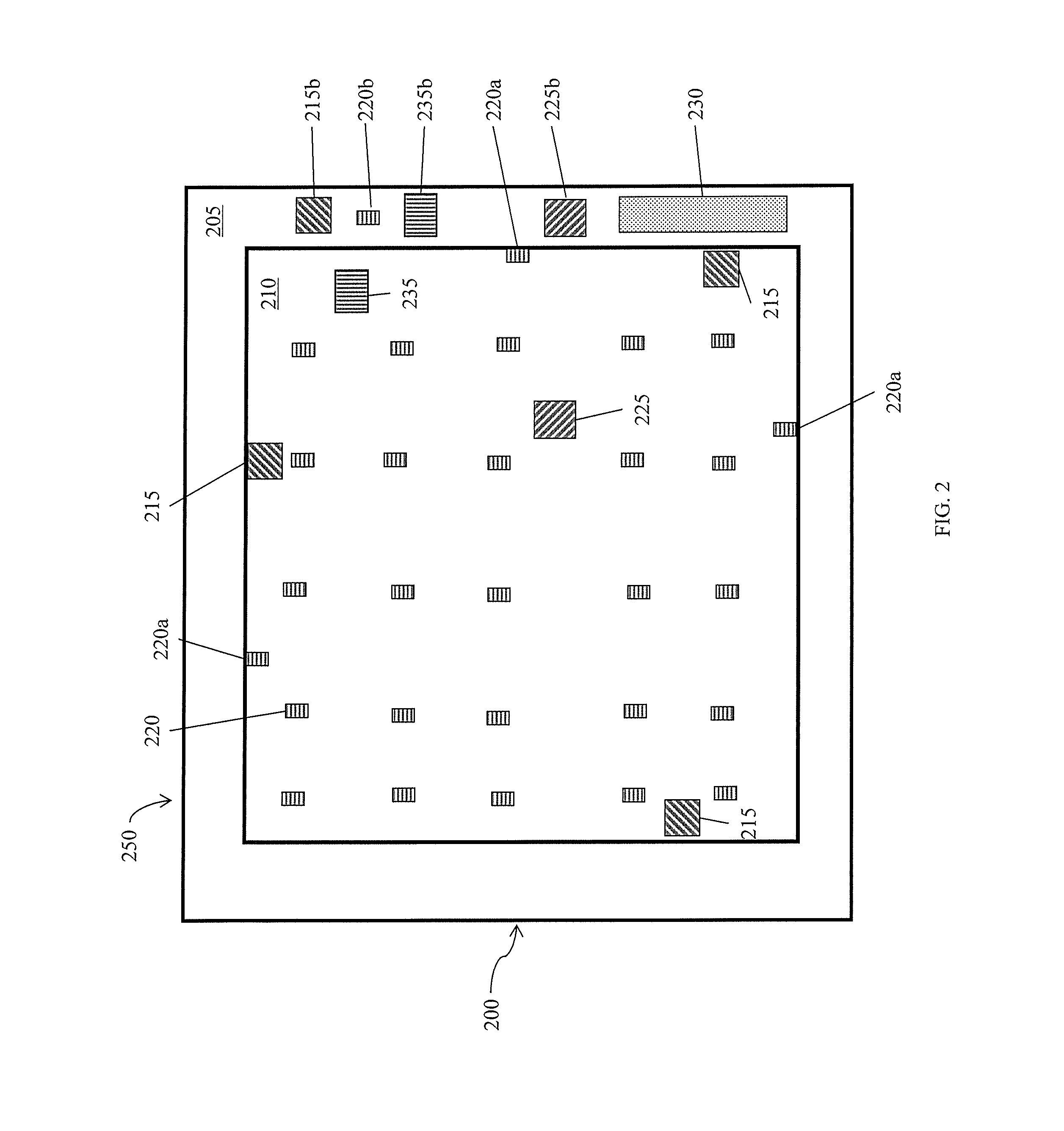
[0014]The invention relates to semiconductor devices and, more particularly, to systems and methods for semiconductor line centering. The present invention can be used to advantageously place substantially identical product disposition macros within product chips and along scribe lines. In this way, the present invention can be used for in-line test and control of the manufacturing process as well as end-of-line test and screen of finished products using macros of substantially identical design.

[0015]The present invention advantageously provides for in-line process control by identifying process-variation induced product-to-scribe line offsets and providing a method to account for these when centering a process for optimum yield to product screen limits. More specifically, according to aspects of the present invention, in-line measurements taken during the manufacturing process can be correlated with measurements of a final product. The correlation between the in-line measurements a...


PUM


Abstract

Methods and systems for semiconductor line scribe centering are provided. A method includes placing and measuring substantially identical test macros within a chip and in a scribe line. The method also includes establishing an estimate correlation between scribe line measurements taken during a manufacturing process and product measurements taken on a final product. The method also includes determining empirical scribe line specification limits consistent with established product screen limits. The method also includes adjusting the manufacturing process in order to optimize performance to the empirical scribe line specification limits.

Description

FIELD OF THE INVENTION[0001]The invention relates to semiconductor devices and, more particularly, to systems and methods for semiconductor line centering.BACKGROUND OF THE INVENTION[0002]Process variation is an increasingly important factor in the design of integrated circuits (ICs) fabricated in advanced semiconductor technologies. Because the precise knowledge of variation is becoming an even more integral part of the design process as technology continues to scale, testing techniques are needed to extract, measure, and characterize variation in a given process and link it to circuit performance.[0003]Process variation in IC fabrication is the deviation from intended or designed values for a structure or circuit parameter of concern. Process variation can result in the fluctuation of parameter values and dimensions in both the structural device and interconnect levels, which can influence the performance of ICs.[0004]In a typical IC manufacturing process, test macros are included...

Claims


Application Information

Patent Timeline
IPC IPC(8): H01L21/66G05B15/02
CPCG05B15/02H01L22/12H01L22/14H01L22/20H01L22/34H01L2924/0002
Inventor BICKFORD, JEANNE P.DEZFULIAN, KEVIN K.GRANINGER, AURELIUS L.HEDBERG, ERIK L.PERRY, TROY J.
Owner GLOBALFOUNDRIES INC
Why Eureka
Try Eureka