

Nitride semicondutor device
a semiconductor and semiconductor technology, applied in the direction of semiconductor devices, electrical apparatus, transistors, etc., can solve the problem of not being able to achieve sufficient electrical conductivity throughout the p-type semiconductor layer, and achieve the effect of sufficient electrical conductivity
- Summary
- Abstract
- Description
- Claims
- Application Information
AI Technical Summary
Benefits of technology
Problems solved by technology
Method used
Image

Examples
first embodiment
[0035](Nitride Semiconductor Device)
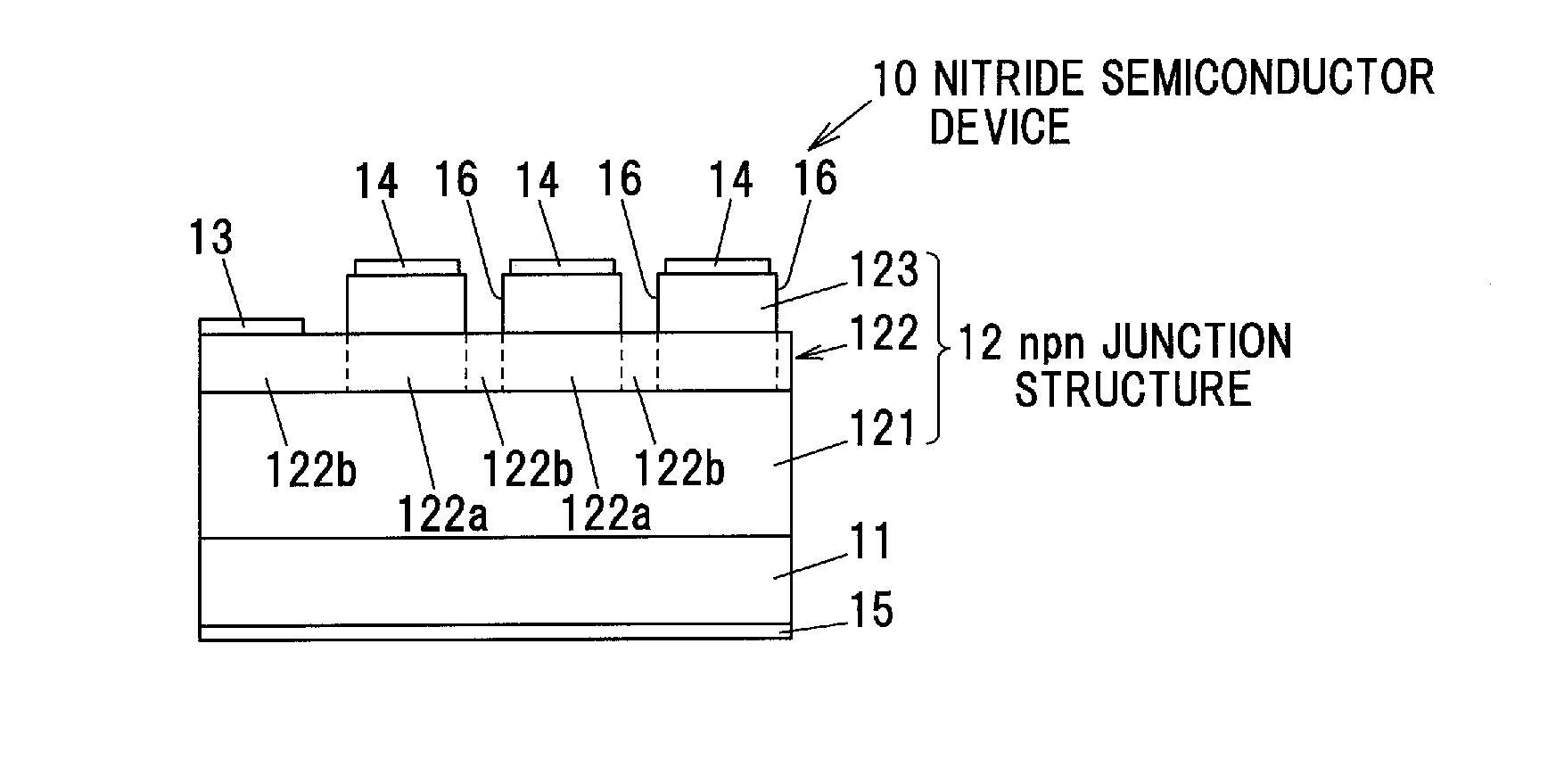
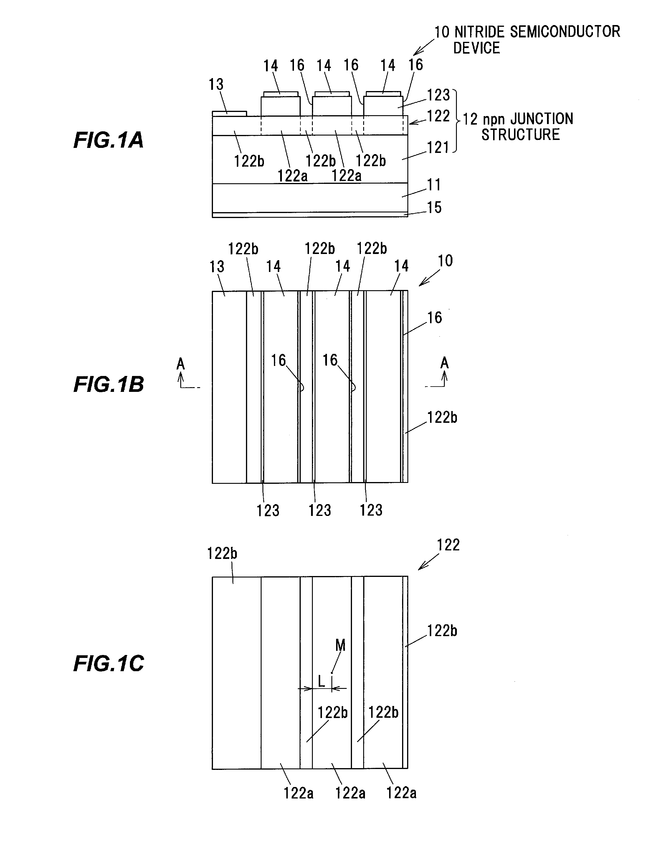
[0036]FIGS. 1A and 1B are diagrams showing a nitride semiconductor device in the first embodiment according to the invention, wherein FIG. 1A is a vertical cross-sectional view thereof, and FIG. 1B is a top view thereof. FIG. 1A is illustrating a cross-sectional view taken along line A-A in FIG. 1B.
[0037]A nitride semiconductor device 10 comprises an n-type nitride semiconductor layer 11, an npn junction structure 12 formed by laminating an n-type nitride semiconductor layer 121, a p-type nitride semiconductor layer 122, and an n-type nitride semiconductor layer 123 sequentially in this order on the n-type nitride semiconductor layer 11, an electrode 13 which is a base electrode electrically connected to the p-type nitride semiconductor layer 122, an electrode 14 which is an emitter electrode electrically connected to the n-type nitride semiconductor layer 123, and an electrode 15 which is a collector electrode electrically connected to the n-type...
second embodiment
[0062](Nitride Semiconductor Device)
[0063]In the second embodiment, the configuration of the emitter electrode is different from that in the first embodiment. The explanation as to the same points as in the first embodiment is omitted or simplified.
[0064]FIGS. 8A and 8B are diagrams showing a nitride semiconductor device in the second embodiment, wherein FIG. 8A is a vertical cross-sectional view thereof, and FIG. 8B is a top view thereof. FIG. 8A is illustrating a cross-sectional view taken along line B-B in FIG. 8B.
[0065]A nitride semiconductor device 20 comprises an n-type nitride semiconductor layer 11, an npn junction structure 12 formed by laminating an n-type nitride semiconductor layer 121, a p-type nitride semiconductor layer 122, and an n-type nitride semiconductor layer 123 sequentially in this order on the n-type nitride semiconductor layer 11, an electrode 13 which is a base electrode electrically connected to the p-type nitride semiconductor layer 122, an electrode 22 ...
example 1
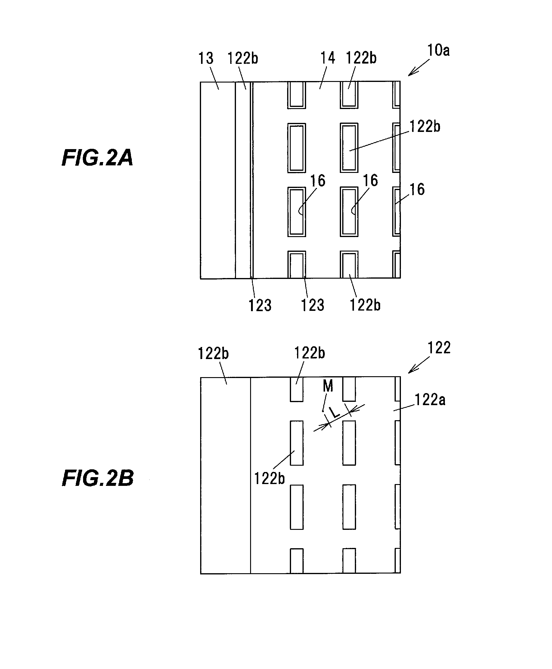
[0079]As Example 1, nitride semiconductor devices 10, 10a, 10b, 10c, and 10d in the first embodiment were prepared and the relationship between the position of the uncovered regions 122b and the residual concentration of hydrogen in the p-type nitride semiconductor layer 122 was examined.
[0080]First, the n-type nitride semiconductor layer 11, the n-type nitride semiconductor layer 121, the p-type nitride semiconductor layer 122, and the n-type nitride semiconductor layer 123 were sequentially formed on the substrate 17 by VAS method to provide a layered structure made of a nitride semiconductor.
[0081]Here, c-plane sapphire substrate of 6 inches (15.24 cm) was used as the substrate 17. Then, a 400 μm-thick n-type GaN sub-collector layer doped with Si at a concentration of about 5×1018 cm−3, a 10 μm-thick n-type GaN collector layer doped with Si at a concentration of about 5×1018 cm−3, a 0.1 μm-thick p-type GaN base layer doped with Mg, and a 0.2 μm-thick n-type GaN emitter layer dope...
PUM
| Property | Measurement | Unit |
|---|---|---|
| distance | aaaaa | aaaaa |
| depth | aaaaa | aaaaa |
| temperature | aaaaa | aaaaa |
Abstract
Description
Claims
Application Information